ADSP-21535 EZ-KIT LITE Evaluation System Manual Second Edition, May 2002 Part Number 82-000603-01 Analog Devices, Inc.
Limited Warranty The EZ-KIT Lite evaluation system is warranted against defects in materials and workmanship for a period of one year from the date of purchase from Analog Devices or from an authorized dealer. Disclaimer Analog Devices, Inc. reserves the right to change this product without prior notice. Information furnished by Analog Devices is believed to be accurate and reliable.
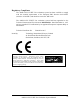
Regulatory Compliance The ADSP-21535 EZ-KIT Lite evaluation system has been certified to comply with the essential requirements of the European EMC directive 89/336/EEC (inclusive 93/68/EEC) and therefore carries the “CE” mark. The ADSP-21535 EZ-KIT Lite evaluation system had been appended to the Technical Construction File referenced ‘DSPTOOLS1’ dated December 21, 1997 and was awarded CE Certification by an appointed European Competent Body as listed below. Technical Certificate No: Issued by: Z600ANA1.
TABLE OF CONTENTS LIST OF TABLES............................................................................................................. vi LIST OF FIGURES ........................................................................................................... vi 1 INTRODUCTION.................................................................................................. 1-1 1.1 For More Information About Analog Devices Products................................. 1-2 1.
4.4.1 Programmable Flag LEDs (LED1, LED2, LED3, LED4) ....................... 4-9 4.4.2 USB Monitor LED (LED5) ...................................................................... 4-9 4.4.3 Power LED (LED6).................................................................................. 4-9 4.4.4 Reset LEDs (LED7, LED8)...................................................................... 4-9 4.4.5 Non-Maskable Interrupt Push Button (SW3) ........................................... 4-9 4.4.
LIST OF TABLES Table 1-1: Related DSP Documents ................................................................................ 1-5 Table 1-2: Related VisualDSP++ Documents ................................................................. 1-5 Table 2-1: Minimum PC Configuration........................................................................... 2-2 Table 3-1: EZ-KIT Lite Evaluation Board Memory Map ............................................... 3-2 Table 3-2: SDRAM Default Settings.................
1 INTRODUCTION Thank you for purchasing the ADSP-21535 EZ-KIT Lite evaluation system. The evaluation board is designed to be used in conjunction with the VisualDSP++ development environment to test the capabilities of the ADSP21535 digital signal processor (DSP).
• • • • • • • Analog Devices AD1885 48 kHz AC’97 SoundMAX Codec o Jumper-Selectable Line-In or Mic-In 3.5 mm Stereo Jack o Line-Out 3.
You may also obtain additional information about Analog Devices and its products in any of the following ways: 1.2 • FAX questions or requests for information to (781) 461-3010. • Access the Computer Products Division File Transfer Protocol (FTP) site at 137.71.23.21 or ftp://ftp.analog.com. For Technical or Customer Support You can reach our Customer Support group in the following ways: • Contact your local Analog Devices sales office or an authorized Analog Devices distributor.
DSP programmers who are unfamiliar with Analog Devices Blackfin DSPs can use this manual in conjunction with the ADSP-21535 DSP Hardware Reference and the ADSP-21535 DSP Instruction Set, which describe the DSP architecture and instruction set. DSP programmers who are unfamiliar with VisualDSP++ should refer to the VisualDSP++ Help menu and the VisualDSP++ User’s Guide. For the locations of these documents, refer to section 1.6. 1.5 Manual Contents This manual contains the following information: 1.
To view help on additional ADSP-21535 EZ-KIT Lite features, go to the windows task bar and select Start\Programs\VisualDSP\EZ-KIT Help. The documents in the following tables can be found through online Help or in the Docs folder of your VisualDSP++ installation. For more documentation, please go to http://www.analog.com/technology/dsp/library.html.
2 GETTING STARTED 2.1 Overview This chapter provides the information you need to begin using ADSP-21535 EZ-KIT Lite evaluation system. For correct operation install the software and hardware in the order presented in section 2.4. This chapter has the following sections: 2.2 • Contents of your EZ-KIT Lite Package (Section 2.2) Provides a list of the components that are shipped with this EZKIT Lite evaluation system. • PC Configuration (Section 2.
The EZ-KIT Lite evaluation system contains ESD (electrostatic discharge) sensitive devices. Electrostatic charges readily accumulate on the human body and equipment and can discharge without detection. Permanent damage may occur on devices subjected to high-energy discharges. Proper ESD precautions are recommended to avoid performance degradation or loss of functionality. Store unused EZ-KIT Lite boards in the protective shipping package. 2.
2.4.1 Installing the VisualDSP++ Software This EZ-KIT Lite comes with the latest version of VisualDSP++ for the Blackfin DSP family. You must install this software before installing the EZ-KIT Lite debug software. Insert the VisualDSP++ CD-ROM into the CD-ROM drive. If Auto Run is enabled on your PC, the home screen of the VisualDSP++ install wizard will automatically appear. If not, choose Run from the Start menu, and enter D:\Setup.exe in the Open field, where D is the name of your local CD-ROM drive.
2.4.4 Setting Up the EZ-KIT Lite Hardware The EZ-KIT Lite evaluation system contains ESD (electrostatic discharge) sensitive devices. Electrostatic charges readily accumulate on the human body and equipment and can discharge without detection. Permanent damage may occur on devices subjected to high-energy discharges. Proper ESD precautions are recommended to avoid performance degradation or loss of functionality. Store unused EZ-KIT Lite boards in the protective shipping package.
3. Plug the provided power supply into P10 on the EZ-KIT Lite board. Visually verify that the green power LED (LED6) is on. Also verify that the two red reset LEDs (LED7 and LED8) go on for a moment and then go off. 4. Connect the USB cable to an available full speed USB Port and to P7 on the ADSP-21535 EZ-KIT Lite board. 2.4.5 Installing the EZ-KIT Lite USB Driver The EZ-KIT Lite evaluation system can be installed on Windows 98 and Windows 2000 and requires one full-speed USB port. Section 2.4.5.
2. Click Next. 3. Select Search for the best driver for your device as shown in Figure 2-3. Figure 2-3: Search for the driver 4. Click Next. 5. Select CD-ROM drive as shown in Figure 2-4. Figure 2-4: Search the CD-ROM 6. Click Next.
Windows 98 will locate the WmUSBEz.inf file that is on the CD-ROM as shown in Figure 2-5. Figure 2-5: The driver is located 7. Click Next. The Coping Files dialog box appears (Figure 2-6). Figure 2-6: Search for .sys File Dialog Box 8. Click Browse.
Figure 2-7 will appear. Figure 2-7: Open the .sys File 9. In Drives select your CD-ROM drive. 10. Click OK. Figure 2-8 will appear. Figure 2-8: Copying Files 11. Click OK.
The driver installation is now complete as shown in Figure 2-9. Figure 2-9: Finish the Software Installation 12. Click Finish to exit the wizard. Verify the installation by following the instructions in section 2.4.6.
2.4.5.2 Windows 2000 USB Driver Installation Before using the ADSP-21535 EZ-KIT Lite for the first time, the Windows 2000 USB driver must first be installed. To install the USB Driver: 1. Insert the EZ-KIT Lite CD-ROM into the CD-ROM drive. The connection of the device to the USB port will activate the Windows 2000 “Found New Hardware Wizard” as shown in Figure 2-10. Figure 2-10: Found New Hardware Wizard 2. Click Next.
3. Select Search for a suitable driver for my device as shown in Figure 2-11. Figure 2-11: Search for a Suitable Driver 4. Click Next.
5. Ensure that CD-ROM drives is selected as shown in Figure 2-12. Figure 2-12: Locate Driver Files 6. Click Next.
Figure 2-13 appears. Figure 2-13: Driver File Search Results 7. Click Next.
Windows 2000 will automatically install the ADSP-21535 EZ-KIT Lite driver. The driver installation is now complete as shown in Figure 2-14. Figure 2-14: Completing Driver Installation Dialog Box 8. Click Finish to exit the wizard. Verify the installation by following the instructions in section 2.4.6. 2.4.6 Verifying Driver Installation Before you use the EZ-KIT Lite evaluation system, verify that the USB driver software is installed properly: 1.
2.4.7 Starting VisualDSP++ To start debugging, set up a session in VisualDSP++. 1. Verify that the yellow USB monitor LED (LED5, located near the USB connector) is lit. This signifies that the board is communicating properly with the host PC, and is ready to run VisualDSP++. 2. Hold down the Control (CTRL) key. 3. Select the Start button on the Windows taskbar, and then choose Programs\VisualDSP\VisualDSP++. The Session List dialog box appears if you already have existing sessions.
3 USING THE EZ-KIT LITE 3.1 Overview This chapter provides specific information to assist you with developing programs for the ADSP-21535 EZ-KIT Lite board. This information appears in the following sections: • EZ-KIT Lite License Restrictions (Section 3.2) Describes the restrictions of the VisualDSP++ license shipped with the EZ-KIT Lite. • Memory Map (Section 3.3) Defines the memory map to assist in developing programs for the EZ-KIT Lite evaluation system. • Using the SDRAM Interface (Section 3.
3.2 EZ-KIT Lite License Restrictions The license shipped with the EZ-KIT Lite imposes the following restrictions: • • • 3.3 Internal Memory space is limited to 176 KB of the ADSP-21535 internal memory space No connections to Simulator or Emulator sessions are allowed. Only one EZ-KIT Lite can be connected to the host PC and debugged at a time Memory Map The ADSP-21535 has internal SRAM that can be used for instruction storage or data storage.
3.4 Using the SDRAM Interface In order to use the 4M x 32 bits (16 MB) of SDRAM memory, the three SDRAM control registers must be initialized. The following table shows the standard configuration for these registers when using the EZ-KIT Lite in the default configuration. These numbers were derived using the M48LC4M16ATG-75 with a system clock frequency of 120 MHz.
0x200A 0000 Main Flash Array 0x2002 0000 Empty 0x2001 00FF Config 0x2001 0000 Empty 0x2000 8000 0x2000 0000 Boot Flash Array Figure 3-1: Flash Memory Map Use PSDsoft ExpressTM to modify the default settings for the flash memory, the DSM project must be modified and the flash must be reprogrammed using FlashLINKTM. The default project files can be found in, \…\VisualDSP\Blackfin\EZ-KITs\ADSP-21535\DSMConfigFiles.
3.6 Using the Programmable Flag Pins The ADSP-21535 has 16 asynchronous Programmable Flag (PF) I/O pins. During reset PF0-PF9 function as inputs to the internal PLL of the DSP. They are not valid until 120uS after reset. Table 3-3 describes how the PFs are used on the EZ-KIT Lite. After a DSP reset, all of the PF pins are initialized as inputs. The direction of the PF is configured by the FIO_DIR Memory Mapped Register (MMR).
3.6.1 Using the Power Management Features PF14-PF12 allow you to program the core voltage of the DSP. The default core voltage is 1.5V. Table 3-4 gives the value of the core voltage corresponding to the state of these PFs. When lowering the core voltage of the DSP, the frequency of the DSP must be taken into consideration. As you lower the core voltage of the DSP, the frequency the core is running at must be decrease.
4 EZ-KIT LITE HARDWARE REFERENCE 4.1 Overview This chapter describes the hardware design of the ADSP-21535 EZ-KIT Lite board. The following topics are covered: • System Architecture (Section 4.2) Describes the configuration of the DSP as well as a description of how all of the components on the board interface with the DSP. • Jumper and DIP Switch Settings (Section 4.3) Shows the location and describes the function of all the configuration jumpers and DIP Switches. • LEDs and Push Buttons (Section 4.
System Architecture The EZ-KIT Lite has been designed to demonstrate the capabilities of the ADSP21535 DSP. This section describes the DSP’s configuration on the EZ-KIT Lite board. JTAG Header 544KB Flash (U4) 4M X 32bit SDRAM (U5, U6) JTAG Port EZ USB FX USB Connector SRAM 20MHz Oscillator External Bus Interface Unit Power Management UART1:0 Timer2:0 ADSP-21535 SPORT1 DSP RTC (U1) USB Expansion Connectors (P1, P2, P3) VDD_INT 3.
4.2.1 External Bus Interface The External Bus Interface Unit (EBIU) is connected to 4M x 32 bits of SDRAM (16 MB). This memory is connected to the synchronous memory select 0 (~SMS0) pin. Refer to section 3.4 for information about configuring the SDRAM. The EBIU is also connected to 272K x 16 bits of flash memory. This memory is connected to the asynchronous memory select (~AMS0) pin. The DSP can use this memory both for booting and storing information during normal operation. Refer to section 3.
4.2.3 Expansion Interface The expansion interface consists of the footprints for 3 connectors. The following table shows the interfaces each connector provides. For the exact pin-out of these connectors refer to APPENDIX B: SCHEMATIC. Analog Devices does not populate these connectors or provide any additional support for this interface. The mechanical locations of these connectors can be found in section 4.6.3. Table 4-1: Connector Interfaces Connector Interfaces P1 5V, GND, Address, Data P2 3.
4.3 Jumper and DIP Switch Settings This section describes the function of all the jumpers and DIP switches. The following figure shows the location of all the jumpers and DIP switches. Figure 4-2: Jumper Locations 4.3.1 Audio Input Select Jumper (JP1) The audio input jack (P5) can be connected to the MIC1 or the LINEIN input channels of the AD1885 Codec (U7). When the JP1 jumpers connect pins 1 and 3 and pins 2 and 4, P3 connects to the mono MIC1 channel.
MIC LINE MIC JP1 6 5 2 1 JP1 2 1 LINE Mono MIC1 Stereo LINE_IN (DEFAULT) 6 5 Figure 4-3: Audio Input Jumper Settings (JP1) 4.3.2 Audio Codec Disable Jumper (JP2) Placing a jumper between pins 1 and 2 of JP2 holds the AD1885 in reset, preventing it from driving signals to the serial port. When a jumper is between pins 2 and 3 of JP2, the AD1885 is held in reset until PF15 is set to an output and is asserted. These position are labeled on the board as “DIS” and “ENA 1885”. 4.3.
During reset, the function of these pins is to setup the PLL. At this time, these signals are attached to the PLL setup switch (SW2) and determine the core and external clock speeds of the DSP. Approximately 120uS after reset has been deasserted these pins are no longer attached to SW2, but function as PFs. The following table shows the switch position that corresponds to a DSP pin.
4.4 LEDs and Push Buttons This section describes the function of all the LEDs and push buttons. Figure 4-5 shows the location of all the LEDs and push buttons.
4.4.1 Programmable Flag LEDs (LED1, LED2, LED3, LED4) Four LEDs are connected to four of the DSP’s Programmable Flag (PF) pins, PF0-3. These LEDs are active HIGH and are lit by an output of “1” from the DSP. Refer to section 3.6 for more information about using of the PFs when programming the DSP. Table 4-4: Programmable Flag LEDs LED Reference Designator LED4 LED1 LED2 LED3 DSP Programmable Flag Pin PF0 PF1 PF2 PF3 4.4.
4.4.6 Programmable Flag Push Buttons (SW4, SW5, SW6, SW7) Four push buttons are provided for general-purpose user input. SW4-7 connect to the DSP’s Programmable Flag (PF) pins, PF4-7. The push buttons are active high and when pressed send a high (1) to the DSP. Refer to section 3.6 for more information about the use of the PFs when programming the DSP. Table 4-5 shows the PF signal and the switch it is connected to.
4.5 Connectors This section describes the function of the connectors and gives information about mating connectors. The following figure shows the locations of the connectors.
4.5.1 Expansion Interface (P1, P2, P3) Three board-to-board connector footprints provide the signals for most of the DSP peripheral interfaces. Analog Devices does not populate these connectors or provide any additional support for this interface. See section 4.2.3, for more information on the Expansion Interface. Contact Samtec for the availability and pricing of these connectors. Part Description 90 Position 0.05” Spacing (P1, P2, P3) Manufacturer Samtec Mating Connector Samtec 90 Position 0.
4.5.4 USB (P7) The USB connector is a standard Type B USB receptacle. This connector is used to debug the DSP, and is not connected to the DSP’s USB interface. Part Description Type B USB receptacle (P7) Manufacturer Mill-Max Digi-Key Mating Connector USB cable (provided with kit) Assmann Digi-Key Part Number 897-30-004-90-000 ED90003-ND AK672-5 AK672-5ND 4.5.5 JTAG (P8) The JTAG header is the connecting point for a JTAG in-circuit emulator pod.
4.5.6 SPORT0 (P9) SPORT0 is connected to a 20-pin connector. The pinout for this connector can be found in APPENDIX B: SCHEMATIC. Contact AMP for pricing and availability on these connectors.
4.6.1 Power Supply The power connector supplies DC power to the EZ-KIT Lite board. Table 4-6 shows the power connector pinout. Table 4-6: Power Connector Terminal Center pin Outer Ring Connection +7.5 VDC@2amps GND 4.6.2 Board Current Measurements The ADSP-21535 EZ-KIT Lite board provides eight zero-ohm resistors that may be removed to measure current draw. Table 4-7 shows the resistor number, the voltage plane, and a description of the components on the plane.
4.6.3 Mechanical Dimensions The following figure shows the location of the mounting holes as well as the PIN1 of each of the expansion connectors. 5.000 4.750 3.875 P1 3.750 2.500 P2 1.400 1.300 1.125 P3 6.750 7.000 6.375 6.200 3.600 3.250 0.625 0.000 0.250 0.250 0.
APPENDIX A: BILL OF MATERIALS REF QTY. 2 3 3 1 4 1 5 1 6 1 7 1 8 1 9 1 10 3 11 1 12 1 13 1 14 1 15 1 16 2 17 1 18 1 19 1 20 2 21 2 22 1 23 1 Description 74LVC14A SOIC14 HEX-INVER-SCHMITT-TRIGGER IDT74FCT3244APY SSOP20 3.3V-OCTAL-BUFFER 24.
24 2 25 1 26 1 27 1 28 5 29 1 30 1 31 1 32 6 33 1 34 1 35 1 36 23 37 2 38 5 39 2 40 79 41 1 42 5 43 4 44 44 45 44 46 4 47 5 48 1 ADP3338AKC-33 SOT-223 3.3V-1.0AMP REGULATOR ADP3339AKC-5 SOT-223 5V-1.5A REGULATOR ADP3088 MSOP8 500MA-BUCK-REGULATOR ADSP-21535PKB-300 PBGA260 308KBYTES-BLACKFIN RUBBER FEET BLACK PWR 2.5MM_JACK CON005 RA USB 4PIN CON009 USB .
49 1 50 1 51 3 52 4 53 1 54 5 55 1 56 3 57 8 58 1 59 2 60 6 61 6 62 2 63 3 64 1 65 1 66 1 67 1 68 1 69 1 70 1 71 1 72 1 73 1 74 3 1.5K 100MW 5% 805 22uF 16V 10% D TANT 2.21K 1/8W 1% 1206 10uF 16V 10% B TANT 1A HSM160J DO-214AA SCHOTTKY 100 100MW 5% 805 1000 100MHZ 1.5A FER002 0.06 CHOKE 2A S2A_RECT DO-214AA SILICON RECTIFIER 600 100MHZ 500MA 1206 0.70 BEAD 0.
75 2 76 5 77 1 78 6 79 1 80 1 81 3 82 7 83 4 84 1 85 1 86 2 87 1 88 5 89 5 90 1 91 1 92 1 93 3 94 1 95 2 39PF 50V 5% 805 NPO 10K 100MW 2% RNET16 BUSSED 1K 1/8W 5% 1206 10K 1/8W 5% 1206 100K 1/8W 5% 1206 20.0K 1/8W 1% 1206 22 1/8W 5% 1206 270 1/8W 5% 1206 4.
APPENDIX B: SCHEMATIC ADSP-21535 EZ-KIT Lite Evaluation System Manual E
A B C D 1 1 2 2 ADSP-21535 EZ-KIT LITE 3 3 ANALOG DEVICES 4 Approvals Drawn Checked Engineering A B C Date Title 20 Cotton Road Nashua, NH 03063 4 PH: 1-800-ANALOGD ADSP-21535 EZ-KIT LITE - TITLE 5/11/02 Size Board No. C Date Rev A0162-2000 1.
A B PWR_MGT_OUT 3V_DSP C D VDD_INT VDD_RTC R2 0.00 1206 R6 0.00 1206 3V FOR RTC 3V_DSP 3V_DSP VDD_EXT RN2 1.5V XTALI VDD_PLL R3 0.00 1206 1 VDD_PCIEXT Y1 32.768KHZ OSC007 R4 33 805 U2 1OE R7 0.00 1206 RN1 XTALO R1 10K 805 R8 0.
A B 3V C D 3V 1 1 RN3 512 KB MAIN FLASH 32KB SECONDARY FLASH RN4 PB0 1R1 COM16 PB1 2R2 R1515 PB2 3R3 R1414 PB3 4R4 R1313 PB4 5R5 R1212 PB5 6R6 R1111 PB6 7R7 R1010 PB7 8R8 R99 PA0 1R1 COM16 PA1 2R2 R1515 PD1 PA2 3R3 R1414 PD3 PA3 4R4 R1313 PA4 5R5 R1212 PA5 6R6 R1111 PA6 7R7 R1010 PA7 8R8 R99 PE7 PD0 10K RNET16 3AD0 PF031 D0 PC7 ~ABE3/SDQM3 4AD1 PF132 D1 PE6 A[21:2] A2 5AD2 PF233 D2 A3 6AD3 PF334 D3 A4 7AD4 PF435 D4 A5 10AD
A B C D SJ2 SHORTING JUMPER DEFAULT=4 & 6 1 AUDIO CODEC AD1885 A5V CT4 10UF B 3V 1 SJ1 SHORTING JUMPER DEFAULT=3 & 5 C8 0.1UF 1206 POPULATE TO COMPLY WITH PC99 R21 0.00 1206 * Analog Signals C114 0.22UF 805 C11 270PF 805 ALT_VAL=1K JP1 SETTINGS SJ1 SJ2 U7 1&3 2&4 MIC IN 3&5 4&6 LINE IN * Denotes Default Setting 25AVDD1 VDD11 38AVDD2 VDD29 43AVDD3 C7 0.01UF 1206 DNP INPUT SOURCE Digital Signals VSS14 26AVSS1 VSS27 40AVSS2 FER2 600 1206 R29 4.
A B C D 3V RN5 1 1R1 BMODE0 U9 COM16 MUL_SEL BMODE1 2R2 R1515 MS5 BMODE2 3R3 R1414 MS6 MS0 4R4 R1313 DF MS1 5R5 R1212 SSEL0 MS2 6R6 R1111 SSEL1 MS3 7R7 R1010 MS4 8R8 R99 MS_PF[0:6] MS_PF1 4 YA 7 YB BYPASS MS_PF2 10K RNET16 MS_PF3 9 YC 12 YD 9 I0A2 MS0 I1A3 PF0 I0B5 MS1 I1B6 PF1 I0C11 MS2 I1C10 PF2 I0D14 MS3 I1D13 PF3 S1 I0D14 DF I1D13 PF7 MS5 6 19 MS6 7 18 DF 8 17 SSEL0 9 16 SSEL1 10 15 11 14 12 13 12 S1 20 BYPASS
A B C D 3V R83 10K 805 PF4 R82 100 805 R63 0.00 1206 U10 9 1 SW4 SWT013 SPST-MOMENTARY 8 3V PF4 74LVC14A SOIC14 1 CT9 1UF A 3V 3V USB RESET LED7 RED-SMT LED001 R90 10K 805 3V RESET LED8 RED-SMT LED001 3V 9 USB_CONFIGURED PF5 USB_RESET R64 0.
A B C D D[0:31] A[2:25] 3V 5V 1 1 1.
A B C D 1 PF14 PF13 1 1 1 1 0 0 0 0 1 1 0 0 1 1 0 0 PF12 VDD_INT 1 0 1 0 1 0 1 0 1.6V 1.5V 1.4V 1.3V 1.2V 1.1V 1.0V 0.9V 1 * * = DEFAULT WAIT 100uS FOR VOLTAGE TO SETTLE AFTER CHANGING PF11-9 UNREG_IN PWR_MGT_OUT L1 10UH IND001 3V_DSP VR5 2 C22 1UF 805 1IN1 SW8 2IN2 DRV7 3GND1 GND26 4COMP FB5 R95 53.6K 805 C21 470PF 1206 R97 0.
A B C D 1 1 5V F1 2.5A FUS001 FER9 CHOKE_COIL FER002 4 3 1 D2 2A DO-214AA UNREG_IN 3INPUT 2 1 2 OUTPUT2 GND 1 ADP3339AKC-5 SOT-223 P10 D3 2A DO-214AA C26 1000PF 1206 R110 0.00 RC05 VR4 R109 100K 1206 CT16 10UF C C27 0.1UF 805 CT17 10UF C C28 0.1UF 805 5V A5V 3 7.5V_POWER CON005 FER6 600 1206 C25 1000PF 1206 R112 0.00 1206 SHGND 2 2 AGND 3V 5V 3V_DSP R113 0.00 1206 VR2 3INPUT FER7 600 1206 5V R111 0.
A B C D 3V 3V 1 C48 0.01UF 805 C47 0.01UF 805 C44 0.01UF 805 C45 0.01UF 805 C46 0.01UF 805 C50 0.01UF 805 C49 0.01UF 805 C54 0.01UF 805 C55 0.01UF 805 MT48LC4M16 (U5) C53 0.01UF 805 3V C52 0.01UF 805 C51 0.01UF 805 C56 0.01UF 805 C57 0.01UF 805 C102 0.01UF 805 C43 0.01UF 805 C42 0.01UF 805 1 MT48LC4M16 (U6) PSD4135 (U4) VDD_INT C93 10UF 1210 C95 10UF 1210 C98 10UF 1210 C82 0.01UF 805 C81 0.01UF 805 C78 0.01UF 805 2 VDD_EXT C79 0.01UF 805 C80 0.01UF 805 C83 0.
INDEX architecture......................................... 4-2 audio................................................. 4-12 audio............................... See SPORT0 expansion .... See connectors:P1,P2,P3 JTAG...................................See JTAG IO voltage........................................... 4-2 B J boot mode select ................................ 4-6 JTAG.........................................4-4, 4-13 jumpers............................................... 4-5 default settings .
SW7.......................................3-5, 4-10 SW8.............................................. 4-10 S SDRAM ......................................3-2, 3-3 SPORT0 ....................................4-3, 4-14 audio codec disable ........................ 4-6 switches.............................................. 4-8 default settings ............................... 2-4 SW1................................................ 4-6 SW2.........................................4-2, 4-6 SW3......................