
user manual

4.2.3 Expansion Interface
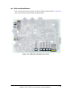
The expansion interface consists of the footprints for 3 connectors. The following
table shows the interfaces each connector provides. For the exact pin-out of these
connectors refer to APPENDIX B: SCHEMATIC. Analog Devices does not
populate these connectors or provide any additional support for this interface.
The mechanical locations of these connectors can be found in section 4.6.3.
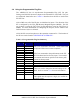
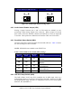
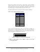
Table 4-1: Connector Interfaces
Connector Interfaces
P1 5V, GND, Address, Data
P2 3.3V, GND, EBUI control signals, PF0-15, SPI0-1, SPORT1,
UART0-1, TMR0-2, NMI
P3 1.5V, GND, Reset, USB, CLKOUT, SLEEP
Limits to the current and to the interface speed must be taken into consideration if
you use this interface. The maximum current limit is dependent on the regulator
used and its capabilities. Additional circuitry can also add extra loading to
signals, decreasing their maximum effective speed.
! Analog Devices does not support and is not responsible for the effects of
additional circuitry.
4.2.4 JTAG Emulation Port
The JTAG emulation port allows an emulator to access the DSP’s internal and
external memory through a 6-pin interface. The JTAG emulation port of the DSP
is also connected to the USB debugging interface (NOTE: This is not the DSP’s
USB interface). When an emulator is connected to the board at P8, the USB
debugging interface is disabled. See section 4.5.5 for more information about the
JTAG connector.
To learn more about available emulators, contact Analog Devices (see section
1.1).
ADSP-21535 EZ-KIT Lite Evaluation System Manual
4-4