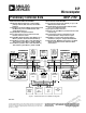
a DSP Microcomputer ADSP-2192 Preliminary Technical Data ADSP-2192 DUAL-CORE DSP FEATURES 320 MIP Dual ADSP-219x DSP in a 144-lead LQFP package with PCI, USB, Sub-ISA, and CardBus Interfaces 3.3V/5V PCI 2.2 Compliant 33MHz / 32-bit Interface with Bus Mastering over four DMA Channels with Scatter-Gather Support Integrated USB 1.
RY For current information contact Analog Devices at (781) 461-3881 A ADSP-2192 October 2000 N L I M A ADSP-219X • 48K words of on-chip RAM on P1, configured as 32K LI DSP ICCORE FEATURES (CONTINUED) E words on-chip 16-bit RAM for Data Memory and 16K N Context Switch Between Two Sets of H P• RSingle-Cycle words on-chip 24-bit RAM for Program Memory A C Computational E ATand DAG Registers T • 4K words of additional on-chip RAM shared by both • Parallel Execution of Computation and Memory D cores, configured
RY For current information contact Analog Devices at (781) 461-3881 A October ADSP-2192 N 2000 I L M A I program Land tors, IC sequencer make the ADSP-2192 more accumulators, which help with overflow. The shifter perE Neven forms logical and arithmetic shifts, normalization, flexible H and easier to program than the R P ADSP-218x A C denormalization, and derive exponent operations. The DSPs.
RY For current information contact Analog Devices at (781) 461-3881 A ADSP-2192 October 2000 N L I M A DSP Peripherals Architecture The programmable interval timer generates periodic interLI NIC E rupts. A 16-bit count register (TCOUNT) is decremented onH page 1 shows the DSP’s on-chip peripherals, R 1C PFigure every n cycles where n-1 is a scaling value stored in a 16-bit A which E include the T Host port (PCI or USB), AC’97 port, register (TSCALE).
RY For current information contact Analog Devices at (781) 461-3881 A October ADSP-2192 N 2000 I L M A LI NItoCgenerate a 24-bit address for each bus. The Table 2 on page 5 shows the interrupt vector and mechanisms E DSP-to-DSP semaphores at reset of each of the peripheral has that support access to the full Hthree functions PRDSP A C The peripheral interrupt’s position in the memory map. T A generate 24-bit addresses for data fetches interrupts.
RY For current information contact Analog Devices at (781) 461-3881 A ADSP-2192 October 2000 N L I M A I Table 2.LDSP-to-DSP Table 3.
RY For current information contact Analog Devices at (781) 461-3881 A October ADSP-2192 N 2000 I L M A I HostIInterface C L2.2 PCI AC’97 2.1 External Codec Interface E N R ADSP-2192 a 33MHz, 32 bit bus master PCI The industry standard AC’97 serial interface (AC-Link) P The Aincludes with CHthat isTcompliant E interface revision 2.2 of the PCI specincorporates a 7-pin digital serial interface that links comA interface supports the high data rates. Tification.DThis pliant codecs to the ADSP-2192.
RY For current information contact Analog Devices at (781) 461-3881 A ADSP-2192 October 2000 N L I M A DSP Core DSP memory accesses use BAR2 or BAR3 of each funcLI Register ICSpace E tion. BAR2 is used to access 24-bit DSP memory; BAR3 N an internal register that is accessible with no R DSPChas H PEach 16-bit DSP memory. Maps of the BAR2 and A latency.
RY For current information contact Analog Devices at (781) 461-3881 A October ADSP-2192 N 2000 I L M A LI transferring When IC samples to and from DSP memory, the Scatter-gather DMA uses four registers. In scatter-gather E N PCI DMA controller R H A can be programmed to perform scat- mode the functions of the registers are mapped as follows: P ter-gather C DMA. T This mode allows the data to be split up Table 4.
RY For current information contact Analog Devices at (781) 461-3881 A ADSP-2192 October 2000 N L I M A I Interrupt Table 5.
RY For current information contact Analog Devices at (781) 461-3881 A October ADSP-2192 N 2000 I L M A LI accesses register or memory location within the ADSP-2192. SimiTarget ICto registers and DSP memory can go E Nfunction. larly, if IO Space access enable is set, then PCI I/O accesses throughH any As long as the Memory Space access R P enable A C can be performed via BAR4.
RY For current information contact Analog Devices at (781) 461-3881 A ADSP-2192 October 2000 N L I M A I Configuration Table 7.
RY A October IN 2000 L M A I C L E HNI R P EC TA T DA For current information contact Analog Devices at (781) 461-3881 ADSP-2192 PCI DWORD BYTE3 BYTE2 BYTE1 BYTE0 PCI Byte Address DSP Word Address 0x0 0000 0x0000 BYTE3 IS ALWAYS UNUSED. BYTE0 IS UNUSED BY 16-BIT MEMORY LOCATIONS. 16K x 24-bit Block 0x0 FFFC 0x1 0000 UNUSED ALLOWED BYTE ENABLES: C/BE = 0000 C/BE = 1000 0x3FFF 0x4000 16K x 16-bit Block UNUSED 0x1 FFFC 0x7FFF Figure 4.
RY For current information contact Analog Devices at (781) 461-3881 A ADSP-2192 N L I A Map (BAR2) IMDSP IMemory 24-bit PCI C L NPCI Address Footprint for the ADSP-2192 Complete RE H PThe C DSP Memory SpacesAin 24-bit (BAR 2) Mode is as follows: TE DAT Table 8.
RY For current information contact Analog Devices at (781) 461-3881 A October N 2000 I L A IM C L Table 8.
RY For current information contact Analog Devices at (781) 461-3881 A ADSP-2192 N L I A Memory Map (BAR 3 Mode) (Continued) IM PCI Table 9.
RY For current information contact Analog Devices at (781) 461-3881 A October N 2000 I L A IM C L 16-bit PCI DSP I/O Memory Map (BAR4) E HNI R Base Address (BAR 4) allows indirect access P PCI ARegister C T to E the ADSP-2192 Control and DSP Memory. A Indirect Registers TThe DSPDMemory Access Registers accessible ADSP-2192 from BAR4 are as follows: Table 10.
RY For current information contact Analog Devices at (781) 461-3881 A ADSP-2192 N L I M DSP ARegister Definitions (Continued) IUSB Table 11.
RY For current information contact Analog Devices at (781) 461-3881 A October ADSP-2192 N 2000 I L M A LIDSPNMemory USB USB Descriptor Release Number IC Buffer Size Register E R Release Number returned in the GET DEVICE P Indicates Aof the DSP memory buffer assigned to this The CHthe size T E endpoint. DESCRIPTOR command is contained in this register.
RY For current information contact Analog Devices at (781) 461-3881 A ADSP-2192 N L I M MCU ARegister Definitions (Continued) IUSB Table 12.
RY For current information contact Analog Devices at (781) 461-3881 A October ADSP-2192 N 2000 I L M A LIEndpoint USB USB Endpoint 3 Code Download Base Address ICDescription Register E N Register R H description endpoint register provides the USB core P The A C T This register contains an 18 bit address which corresponds E information about the endpoint type, direction, and Twith DAsize. This register is read/write by the MCU to the starting location for DSP code download on max packet only.
RY For current information contact Analog Devices at (781) 461-3881 A ADSP-2192 October 2000 N L I M A USB SETUP • INT = Active interrupt for the 8052 MCU LI Counter IC Register E N • ISE = Current interrupt is for a SETUP token information as the total size of the R register Hprovides PThis A C setup transaction data stage. This register is read/write by T • IIN = Current interrupt is for an IN token A TE only.
RY For current information contact Analog Devices at (781) 461-3881 A October N 2000 I L A IM C L Table 13. CONFIG DEVICE Device Descriptor (Continued) E HNI R P Offset A C Description TE DAT Field 14 iManufacturer Manufacturer index string ADSP-2192 Value 0x01 15 iProduct Product index string 0x02 16 iSerialNumber Serial number index string 0x00 17 bNumConfigurations Number of configurations = 1 0x01 Table 14.
RY For current information contact Analog Devices at (781) 461-3881 A ADSP-2192 N L I M CDEVICE A ICONFIG Table 17.
RY For current information contact Analog Devices at (781) 461-3881 A October N 2000 I L A IM C L Table 18. USB MCUCODE (Code Download) (Continued) E HNI R P Offset A C Size Value Description TE DAT Field 5 wIndex (H) 1 0x00 6 wLength (L) 1 0xXX1 Length = XX bytes 7 wLength (H) 1 0xYY2 Length = YY bytes 1 XX is user-specified. 2 YY is user-specified. ADSP-2192 Table 19.
RY For current information contact Analog Devices at (781) 461-3881 A ADSP-2192 N L I M REGIO A (Register Read) (Continued) IUSB Table 20. C L I RE CHNField POffset Size Value Description E AT A T D wValue (H) 3 1 XXX Address <8:15> 4 wIndex (L) 1 0x00 5 wIndex (H) 1 0x00 6 wLength (L) 1 0x02 7 wLength (H) 1 0x00 Since there are three possible interfaces supported, each interface has its own DSP download address and uses its own BULK pipe to download code.
RY For current information contact Analog Devices at (781) 461-3881 A October ADSP-2192 N 2000 I L M A I 4. LConfiguration IC specifies which endpoints are used (and Table 22. Typical Configuration for FAX Modem E N their definitions). A typical configuration for ADSL R P Eappears A 21. CH inTTable End Max Comment Type A T5. TheDuser-defined Point Packet driver downloads USB configuration for interface 2, which is the FAX modem. Configuration specifies which endpoints are used and their definitions.
RY For current information contact Analog Devices at (781) 461-3881 A ADSP-2192 October 2000 N L I M A the Endpoint Stall Policy register that can be programmed If for some reason C host sends more data than the maxLI the I thecore E with a value indicating how many NAK's should be sent packetsize, USB accepts it, as long as there is N R Croom H in theAFIFO. Psufficient prior to transmitting a short packet. This allows flexibility T E in determining how IRPs are retired via short packets.
RY For current information contact Analog Devices at (781) 461-3881 A October ADSP-2192 N 2000 I L M A I Deassertion of PDW1 high causes a wake-up of the DSP. AnL active lowIRST input (to be derived from PCI RST and E N Csources) possibleH other and an active-high IRQ interrupt The PME_EN output from the Combo Master should R P output A C are available.
RY For current information contact Analog Devices at (781) 461-3881 A ADSP-2192 October 2000 N L I M A I • SMSel (Bit 3): Stereo / Mono Select - AC’97 Mode When communicating with the AC'97 interface, the ConLEnable ICin the E Only (0 = Mono Stream or 1 = Stereo Stream) nection bits control register are set to '10'. N H PBitR3 selects stereo orA mono transfers to and from the AC'97 C • SLOT (Bits 7–4): AC’97 Slot Select - AC’97 Mode interface.
RY For current information contact Analog Devices at (781) 461-3881 A October ADSP-2192 N 2000 I L M A I Note that PORST is not needed when using PCI or USB • LSMSel (Bit IC3): Stereo / Mono Select - AC’97 Mode E N Only. (0 = Mono Stream or 1 = Stereo Stream) (and is shown as a no connect in Figure 8 on page 33); these R P • ESLOT A7–4): AC’97 Slot Select - AC’97 Mode CH (Bits interfaces reset the DSP under their control as needed. T T Only.DA DSP Software Reset Table 26.
RY A ADSP-2192 IN AL M I EL HNIC R P EC TA T DA October 2000 For current information contact Analog Devices at (781) 461-3881 D S P E M E RG E S F RO M ~R E S E T A ND P R O G RA M F L O W JUM P S T O B O O T R O M L O AD E R K E RN E L R E AD S C RS T P IN S A ND D E TE R M INE S M O DE O F BO O T IN G ; A LS O P E RF O R M S H O U S E KE E P IN G O P E RA T IO N S, S E T T ING U P IN TE R RU P T S, E T C.
RY For current information contact Analog Devices at (781) 461-3881 A October N 2000 I L IM ICA A L manufacturer. parallel-resonant, fundamental frequency, E HN PRmicroprocessor-grade A 24.576 MHz crystal should be used C configuration. forEthis T T DA ADSP-2192 24.576 M Hz X T AL I CL K SE L X T AL O ADSP-2192 BU S 1 BU S S E LE C T BU S 0 P O W E R O N R E SE T (NO CO N NE C T) PORST P CI C L O C K R UN CL K RU N P CI C L O C K CL K P CI R E S ET RS T AC '97 B IT CL O CK BITC LK Figure 8.
RY For current information contact Analog Devices at (781) 461-3881 A ADSP-2192 October 2000 N L I M A Instruction tion-level simulator; a C/C++ compiler; and a C/C++ LI SetNDescription IC E run-time library that includes DSP and mathematical funcassembly language instruction set has an RADSP-2192 H PThe A C algebraic syntax that T was designed for ease of coding and tions. Two key points for these tools are: E A T readability.
RY For current information contact Analog Devices at (781) 461-3881 A October ADSP-2192 N 2000 I L M A LI (a 2Nrow nector IC× 7 pin strip header) such as that shown in The JTAG signals are terminated on the emulator probe E as follows: Figure 10 on 35. The emulator probe plugs directly R H page P onto A C this connector for chip-on-board emulation. You must T A to your target board design if you intend Table 27.
RY A ADSP-2192 IN AL M I EL HNIC R P EC TA T DA October 2000 For current information contact Analog Devices at (781) 461-3881 OTHER JTAG CONTROLLER TRST TMS TDO EMU TDI TCK TCK TDO TRST TDI TMS TDO TRST EMU TMS EZ-ICE JTAG CONNECTOR TDI TCK TDI JTAG DEVICE (OPTIONAL) ADSP-2192 P1 ADSP-2192 P0 TCK TMS EMU TRST TDO CLKIN OPTIONAL Figure 11.
RY For current information contact Analog Devices at (781) 461-3881 A October N 2000 I L A IM C L Table 28.
RY For current information contact Analog Devices at (781) 461-3881 A ADSP-2192 N L I M CAPin Configurations: PCI/USB Bus Interface (Continued) IADSP-2192 Table 28.
RY For current information contact Analog Devices at (781) 461-3881 A October N 2000 I L A IM C L Table 30. Pin Configurations: Analog Pins (Continued) E HNI R P Pin C TA LQFP I/O Description TE Name DA 63 CTRLVDD I Control Vdd IVDD 62 I Digital Vdd NC 66 O No Connect NC 69 I No Connect NC 70 I No Connect RVAUX 60 I X supply RVDD 64 I Analog Vdd supply ADSP-2192 Table 31.
RY For current information contact Analog Devices at (781) 461-3881 A ADSP-2192 N L I M Configurations: A IPin Table 33. Emulator Pins (Continued) C L I E N R Name PPin A I/O Description CH TLQFP E A T D 81 TDO O Emulator Data Output TMS 75 I Emulator Mode Select TRST 79 I Emulator Logic Reset October 2000 Table 34.
RY For current information contact Analog Devices at (781) 461-3881 A October N 2000 I L A IM C L Table 36. Pin Configurations: Power Supply Pins E HNI R P Pin C TA LQFP I/O Description TE Name DA 92 ACVAUX AIOGND 91 AVDD 65 CTRLAUX 61 CTRLVDD 63 IGND 20, 41, 50, 59, 104, 120, 126, 139 IGND 122 IVDD 19, 40, 49, 58, 103, 117, 125, 140 IVDD 62 RVAUX 60 RVDD 64 REV.
RY For current information contact Analog Devices at (781) 461-3881 A ADSP-2192 N L I IM ICA L ADSP-2192—SPECIFICATIONS E N PR ECH TA NoteTthat component DA specifications are subject to change October 2000 without notice. RECOMMENDED OPERATING CONDITIONS Signal K Grade Parameter Min Max Units VDDINT1,2 Internal Supply Voltage 2.38 2.62 V VDDEXT3 External Supply Voltage Option 3.3V (All Supplies) 3.13 3.47 V VDDEXT4 External Supply Voltage Option 5.0V (VDD Supplies only) 4.75 5.
RY For current information contact Analog Devices at (781) 461-3881 A October N 2000 I IM ICAL L E ELECTRICAL CHARACTERISTICS (CONTINUED) N PR ECH TA TParameter Test Conditions Min DA ADSP-2192 Max Units IDD Supply Current Dynamic (Internal) @ 160 MIPS TBD mA IDD-IDLE Supply Current (Idle) VDDINT = 2.5V TBD mA CIN Input Capacitance6, 7 fIN=1 MHz, TCASE=25°C, VIN=2.5V TBD pF 1 Applies to output and bidirectional pins. 2 Applies to input. 3 Applies to input pins with internal pull-ups.
RY For current information contact Analog Devices at (781) 461-3881 A ADSP-2192 N L I M CInterface A ISub-ISA Table 37. Timing Parameters L I E N R CH Description PParameters Min.
RY A October IN 2000 L M A I C L E HNI R P EC TA T DA For current information contact Analog Devices at (781) 461-3881 ADSP-2192 AE N t AESU t RDY2 t RDY1 tAEHD IO CH RD Y tICYC IOW t STW t WDSU t DHD2 IS AD 15 -0 tADSU t ADHD IS AA 3-1 Figure 13. Sub-ISA Interface Write Cycle Timing Diagram REV. PrA RY A IN AL M I EL HNIC R This information applies to a product under development. Its characteristics and specifications are subject Pto changewriting. A Cwith- T45 out notice.
RY For current information contact Analog Devices at (781) 461-3881 A ADSP-2192 N L I IM ICA L RE CHN A POUTPUT AT CURRENTS TE DDRIVE October 2000 The typical I-V characteristics for the output drivers of the ADSP-2192 are TBD. POWER DISSIPATION Total power dissipation for the ADSP-2192 is TBD. TEST CONDITIONS The ADSP-2192 is tested for compliance with all support industry standard interfaces (PCI, USB, and AC’97). Also, the DSP is tested for output enable, disable, and hold time.
RY A October IN 2000 L M A I C L E HNI R P EC TA TADSP-2192 DA 144-LEAD LQFP PINOUT Table 38 lists the LQFP pinout by signal. Table 38. 144-Lead LQFP Pins By Signal For current information contact Analog Devices at (781) 461-3881 Table 38. 144-Lead LQFP Pins By Signal Table 38. 144-Lead LQFP Pins By Signal ADSP-2192 Table 38.
RY A ADSP-2192 IN AL M I Table 38. 144-Lead L ICLQFP PinsE By SignalN PR ECH TA SIGNAL T DA PIN # October 2000 For current information contact Analog Devices at (781) 461-3881 Table 38. 144-Lead LQFP Pins By Signal Table 39. 144-Lead LQFP Pins By Pin # (Continued) Table 39.
RY A October IN 2000 L M A I39. 144-Lead C L Table LQFP E Pin NI# (Continued) Pins ByH R P EC TA TSIGNAL DA PIN # For current information contact Analog Devices at (781) 461-3881 Table 39. 144-Lead LQFP Pins By Pin # (Continued) Table 39.
RY A October IN 2000 L M A I C L E HNI R P EC TA T DA For current information contact Analog Devices at (781) 461-3881 ADSP-2192 22.00 BS C S Q 1.60 M AX 20.00 BS C S Q 0.75 0.60 109 144 0.45 1 108 S E AT IN G P L AN E 0.27 0.22 T O P V IE W (PINS DOWN) 0.17 73 36 0.08 M AX 0.15 0.05 37 1.45 1.40 1.35 72 0.50 B SC NO T E S : AL L D IM E N S IO NS A RE IN M ILL IM E TE RS (m m ). T HE A CT UA L P O S IT IO N O F EA CH L E AD IS W IT H IN 0.