
User manual


P
R
E
L
I
M
I
N
A
R
Y
T
E
C
H
N
I
C
A
L
D
A
T
A
P
R
E
L
I
M
I
N
A
R
Y
T
E
C
H
N
I
C
A
L
D
A
T
A
This information applies to a product under development. Its characteristics and specifications are subject to change with-
out notice. Analog Devices assumes no obligation regarding future manufacturing unless otherwise agreed to in writing.
3REV. PrA
For current information contact Analog Devices at (781) 461-3881
ADSP-2192October 2000
tors, and program sequencer make the ADSP-2192 more
flexible and even easier to program than the
ADSP-218x DSPs.
Indirect addressing options provide addressing flexibility—
premodify with no update, post-modify with update, pre-
and post-modify by an immediate 8-bit, two’s-complement
value and base address registers for easier implementation
of circular buffering.
The ADSP-2192 integrates 64K words of on-chip memory
configured as 32K words (24-bit) of program RAM, and
96K words (16-bit) of data RAM. Power-down circuitry is
also provided to meet the low power needs of battery oper-
ated portable equipment. The ADSP-2192 is available in a
144-lead LQFP package.
Fabricated in a high speed, low power, CMOS process, the
ADSP-2192 operates with a 6.25-ns instruction cycle time
(160 MIPS). All instructions, except two multiword
instructions, can execute in a single DSP cycle.
The ADSP-2192’s flexible architecture and comprehensive
instruction set support multiple operations in parallel. For
example, in one processor cycle, each DSP core within the
ADSP-2192 can:
• Generate an address for the next instruction fetch
• Fetch the next instruction
• Perform one or two data moves
• Update one or two data address pointers
• Perform a computational operation
These operations take place while the processor
continues to:
• Receive and/or transmit data through the Host port
(PCI or USB interfaces)
• Receive or transmit data through the AC’97
• Decrement the two timers
DSP Core Architecture
The ADSP-2192 instruction set provides flexible data
moves and multifunction (one or two data moves with a
computation) instructions. Every single-word instruction
can be executed in a single processor cycle. The
ADSP-2192 assembly language uses an algebraic syntax for
ease of coding and readability. A comprehensive set of
development tools supports program development.
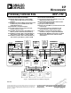
Figure 1 on page 1 shows the architecture of the
ADSP-219x dual-core DSP. Each core contains three inde-
pendent computational units: the ALU, the
multiplier/accumulator (MAC) and the shifter. The compu-
tational units process 16-bit data from the register file and
have provisions to support multiprecision computations.
The ALU performs a standard set of arithmetic and logic
operations; division primitives are also supported. The
MAC performs single-cycle multiply, multiply/add and
multiply/subtract operations. The MAC has two 40-bit
accumulators, which help with overflow. The shifter per-
forms logical and arithmetic shifts, normalization,
denormalization, and derive exponent operations. The
shifter can be used to efficiently implement numeric format
control, including multiword and block floating-point
representations.
Register-usage rules influence placement of input and
results within the computational units. For most operations,
the computational units’ data registers act as a data register
file, permitting any input or result register to provide input
to any unit for a computation. For feedback operations, the
computational units let the output (result) of any unit be
input to any unit on the next cycle. For conditional or mul-
tifunction instructions, there are restrictions on which data
registers may provide inputs or receive results from each
computational unit. For more information, see the
ADSP-219x DSP Instruction Set Reference.
A powerful program sequencer controls the flow of instruc-
tion execution. The sequencer supports conditional jumps,
subroutine calls, and low interrupt overhead. With internal
loop counters and loop stacks, the ADSP-2192 executes
looped code with zero overhead; no explicit jump instruc-
tions are required to maintain loops.
Two data address generators (DAGs) provide addresses for
simultaneous dual operand fetches. Each DAG maintains
and updates four 16-bit address pointers. Whenever the
pointer is used to access data (indirect addressing), it is pre-
or post-modified by the value of one of four possible modify
registers. A length value and base address may be associated
with each pointer to implement automatic modulo address-
ing for circular buffers. Page registers in the DAGs allow
linear or circular addressing within 64 Kword boundaries of
each of the memory pages, but these buffers may not cross
page boundaries. Secondary registers duplicate all the pri-
mary registers in the DAGs; switching between primary and
secondary registers provides a fast context switch.
Efficient data transfer in the core is achieved with the use of
internal buses:
• Program Memory Address (PMA) Bus
• Program Memory Data (PMD) Bus
• Data Memory Address (DMA) Bus
• Data Memory Data (DMD) Bus
Program memory can store both instructions and data, per-
mitting the ADSP-2192 to fetch two operands in a single
cycle, one from program memory and one from data mem-
ory. The DSP’s dual memory buses also let the ADSP-2192
core fetch an operand from data memory and the next
instruction from program memory in a single cycle.