
Datasheet


Data Sheet MAT01
Rev. D | Page 5 of 12
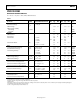
ABSOLUTE MAXIMUM RATINGS
Table 3.
Parameter
1
Rating
Breakdown Voltage of
Collector to Base Voltage (BV
CBO
) 45 V
Collector to Emitter Voltage (BV
CEO
) 45 V
Collector to Collector Voltage (BV
CC
) 45 V
Emitter to Emitter Voltage (BV
EE
) 45 V
Emitter to Base Voltage (BV
EBO
)
2
5 V
Current
Collector (I
C
) 25 mA
Emitter (I
E
) 25 mA
Total Power Dissipation
Case Temperature ≤ 40°C
3
1.8 W
Ambient Temperature ≤ 70°C
4
500 mW
Temperature Range
Operating −55°C to +125°C
Junction −55°C to +150°C
Storage −65°C to +150°C
Lead Temperature (Soldering, 60 sec) 300°C
1
Absolute maximum ratings apply to packaged devices.
2
Application of reverse bias voltages in excess of rating shown can result in
degradation of h
FE
and h
FE
matching characteristics. Do not attempt to
measure BV
EBO
greater than the 5 V rating.
3
Rating applies to applications using heat sinking to control case
temperature. Derate linearity at 16.4 mW/°C for case temperatures above
40°C.
4
Rating applies to applications not using heat sinking; device in free air only.
Derate linearity at 6.3 mW/°C for ambient temperatures above 70°C.
Stresses above those listed under Absolute Maximum Ratings
may cause permanent damage to the device. This is a stress
rating only; functional operation of the device at these or any
other conditions above those indicated in the operational
section of this specification is not implied. Exposure to absolute
maximum rating conditions for extended periods may affect
device reliability.
ESD CAUTION