
Datasheet
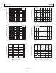
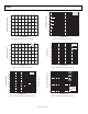


Table Of Contents

Data Sheet OP200
Rev. G | Page 13 of 16
DUAL 12-BIT VOLTAGE OUTPUT DAC
The dual output DAC shown in Figure 33 is capable of providing
untrimmed 12-bit accurate operation over the entire military
temperature range. Offset voltage, bias current, and gain errors
of the OP200 contribute less than 1/10 of an LSB error at 12 bits
over the military temperature range.
DUAL PRECISION VOLTAGE REFERENCE
A dual OP200 and a REF43, a 2.5 V reference, can be used to
build a ±2.5 V precision voltage reference. Maximum output
current from each reference is ±10 mA with load regulation
under 25 μV/mA. Line regulation is better than 15 μV/V and
output voltage drift is under 20 μV/°C. Output voltage noise
from 0.1 Hz to 10 Hz is typically 75 μV p-p. R1 and D1 ensure
correct startup.
00322-033
DAC A
1/2
DAC8221
DAC8221
DAC DATA BUS
PIN 6 (MSB)
TO PIN 17 (LSB)
1/2
OP200AZ
1/2
OP200AZ
OUT A
V–
OUT B
R
FB A
V
DD
I
OUT A
R
FB B
I
OUT B
V
REF A
V
REF B
2
6
1
8
4
7
3
3
21
4
22
2
23
24
AGND
DGND
1
5
18
19
20
10V
REFERENCE
VOLTAGE
5
V
5
DAC B
1/2
DAC8221
DAC
CONTROL
DAC A/DAC B
CS
WR
Figure 33. Dual 12-Bit Voltage Output DAC
0
0322-034
1/2
OP200AZ
REF43
V
OUT
TRIM
GND
V
IN
1/2
OP200AZ
–2.5V
+2.5V
–5V
R1
22kΩ
D1
1N914
1
7
4
8
2
6
6
5
5
4
2
3
R3
10kΩ
+5
V
+5V
R3
10kΩ
R4
5kΩ
Figure 34. Dual Precision Voltage Reference