
Datasheet


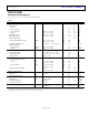

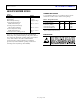


Table Of Contents
- Features
- Applications
- Pin Configurations
- General Description
- Revision History
- Specifications
- Absolute Maximum Ratings
- Typical Performance Characteristics
- Functional Description
- Total Noise-Including Source Resistors
- Gain Linearity
- Input Overvoltage Protection
- Output Phase Reversal
- Settling Time
- Overload Recovery Time
- THD + Noise
- Capacitive Load Drive
- Stray Input Capacitance Compensation
- Reducing Electromagnetic Interference
- Proper Board Layout
- Difference Amplifiers
- A High Accuracy Thermocouple Amplifier
- Low Power Linearized RTD
- Single Operational Amplifier Bridge
- Realization of Active Filters
- Outline Dimensions

Data Sheet OP1177/OP2177/OP4177
Rev. I | Page 5 of 24
ABSOLUTE MAXIMUM RATINGS
Table 3.
Parameter Rating
Supply Voltage 36 V
Input Voltage V
S−
to V
S+
Differential Input Voltage ±Supply Voltage
Storage Temperature Range
R, RM, and RU Packages −65°C to +150°C
Operating Temperature Range
OP1177/OP2177/OP4177 −40°C to +125°C
Junction Temperature Range
R, RM, and RU Packages −65°C to +150°C
Lead Temperature, Soldering (10 sec) 300°C
Stresses at or above those listed under Absolute Maximum
Ratings may cause permanent damage to the product. This is a
stress rating only; functional operation of the product at these
or any other conditions above those indicated in the
operational section of this specification is not implied.
Operation beyond the maximum operating conditions for
extended periods may affect product reliability.
THERMAL RESISTANCE
θ
JA
is specified for the worst-case conditions, that is, a device
soldered in a circuit board for surface-mount packages.
Table 4. Thermal Resistance
Package Type
1
θ
JA
θ
JC
Unit
8-Lead MSOP (RM-8) 190 44 °C/W
8-Lead SOIC_N (R-8) 158 43 °C/W
14-Lead SOIC_N (R-14) 120 36 °C/W
14-Lead TSSOP (RU-14) 240 43 °C/W
1
MSOP is available in tape and reel only.
ESD CAUTION