
Datasheet


REV. B
OP275
–7–
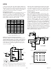
APPLICATIONS
Circuit Protection
OP275 has been designed with inherent short circuit protection
to ground. An internal 30 W resistor, in series with the output,
limits the output current at room temperature to I
SC
+ = 40 mA
and I
SC
– = –90 mA, typically, with ±15 V supplies.
However, shorts to either supply may destroy the device when
excessive voltages or currents are applied. If it is possible for a
user to short an output to a supply, for safe operation, the out-
put current of the OP275 should be design-limited to ± 30 mA,
as shown in Figure 1.
Total Harmonic Distortion
Total Harmonic Distortion + Noise (THD + N) of the OP275
is well below 0.001% with any load down to 600 W. However,
this is dependent upon the peak output swing. In Figure 2, the
THD + Noise with 3 V rms output is below 0.001%. In Figure 3,
THD + Noise is below 0.001% for the 10 kW and 2 kW loads but
increases to above 0.1% for the 600 W load condition. This is a
result of the output swing capability of the OP275. Notice the
results in Figure 4, showing THD versus V
IN
(V rms). This
figure shows that the THD + Noise remains very low until the
output reaches 9.5 V rms. This performance is similar to com-
petitive products.
R
FB
FEEDBACK
R
X
332 ⍀
A1
V
OUT
A1 = 1/2 OP275
–
+
Figure 1. Recommended Output Short Circuit Protection
R
L
= 600
⍀
, 2k
⍀
, 10k
⍀
V
S
=
ⴞ
15V
V
IN
= 3V rms
A
V
= +1
0.010
0.001
0.0005
20 100 1k 10k 20
k
FREQUENCY – Hz
THD + NOISE – %
Figure 2. THD + Noise vs. Frequency vs. R
LOAD
1
0.001
0.0001
20 100 1k 10k 20
k
THD + NOISE – %
FREQUENCY – Hz
A
V
= +1
V
S
= ⴞ18V
V
IN
= 10V rms
80kHz FILTER
600⍀
2k⍀
10k⍀
0.1
0.010
Figure 3. THD + Noise vs. R
LOAD
; V
IN
=10 V rms,
V
S
= ⴞ18V
R
L
= 600⍀
0.010
0.001
0.0001
0.5 1 10
THD + NOISE – %
OUTPUT SWING – V rms
Figure 4. Headroom, THD + Noise vs. Output
Amplitude (V rms); R
LOAD
= 600
⍀
, V
SUP
=
±
18 V
The output of the OP275 is designed to maintain low harmonic
distortion while driving 600 W loads. However, driving 600 W
loads with very high output swings results in higher distortion if
clipping occurs. A common example of this is in attempting to
drive 10 V rms into any load with ± 15 V supplies. Clipping will
occur and distortion will be very high. To attain low harmonic
distortion with large output swings, supply voltages may be
increased. Figure 5 shows the performance of the OP275 driv-
ing 600 W loads with supply voltages varying from ±18 V to ±20 V.
Notice that with ±18 V supplies the distortion is fairly high,
while with ±20 V supplies it is a very low 0.0007%.
SUPPLY VOLTAGE – V
0.0001
0.001
THD – %
0
ⴞ
17
ⴞ
22
ⴞ
18
ⴞ
19
ⴞ
20
ⴞ
21
0.01
0.1
R
L
= 600
⍀
V
OUT
= 10V rms @ 1kHz
Figure 5. THD + Noise vs. Supply Voltage
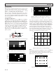
Noise
The voltage noise density of the OP275 is below 7 nV/÷Hz from
30 Hz. This enables low noise designs to have good perfor-
mance throughout the full audio range. Figure 6 shows a typical
OP275 with a 1/f corner at 2.24 Hz.
10Hz
0Hz
CH A: 80.0
V FS
10.0
V/DIV
MKR: 45.6
V/ Hz
BW: 0.145Hz
MKR: 2.24Hz
Figure 6. 1/f Noise Corner, V
S
=
±
15 V, A
V
= 1000