
Datasheet


REV. B
OP275
–9–
+15V
+
0.1F
2
3
8
1
4
V
IN
V
OUT
R
L
2k⍀
–15V
10F
0.1F
1/2
OP275
10F
+
–
+
Figure 12. Unity Gain Follower
0.1
F
+15V
+
10
F
2
3
8
1
4
V
IN
V
OUT
2k
⍀
–15V
10
F
0.1
F
10pF
4.99k
⍀
2.49k
⍀
4.99k
⍀
+
1/2
OP275
–
+
Figure 13. Unity Gain Inverter
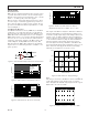
In inverting and noninverting applications, the feedback resis-
tance forms a pole with the source resistance and capacitance
(R
S
and C
S
) and the OP275’s input capacitance (C
IN
), as shown
in Figure 14. With R
S
and R
F
in the kilohm range, this pole can
create excess phase shift and even oscillation. A small capacitor,
C
FB
, in parallel and R
FB
eliminates this problem. By setting R
S
(C
S
+ C
IN
) = R
FB
C
FB
, the effect of the feedback pole is com-
pletely removed.
16V–20V
0.1F
V+
ⴞ5V
R
L
1k⍀
D1 D2
+15V
2N4416
1k⍀
D3
D4
OUTPUT
(TO SCOPE)
1F
10k⍀
IC2
R
F
2k⍀
750⍀
2N2222A
15k⍀
–15V
1N4148
DUT
1/2 OP260AJ
16V–20V
0.1F
10k⍀
–+
+
–
SCHOTTKY DIODES D1–D4 ARE
HEWLETT-PACKARD HP5082-2835
IC1 IS 1/2 OP260AJ
IC2 IS PMI OP41EJ
V–
R
G
222⍀
–
+
–
+
–
+
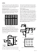
Figure 11. OP275’s Settling Time Test Fixture
R
FB
C
IN
R
S
C
S
C
FB
V
OUT
–
+
Figure 14. Compensating the Feedback Pole
Attention to Source Impedances Minimizes Distortion
Since the OP275 is a very low distortion amplifier, careful atten-
tion should be given to source impedances seen by both inputs.
As with many FET-type amplifiers, the p-channel JFETs in the
OP275’s input stage exhibit a gate-to-source capacitance that
varies with the applied input voltage. In an inverting configura-
tion, the inverting input is held at a virtual ground and, as such,
does not vary with input voltage. Thus, since the gate-to-source
voltage is constant, there is no distortion due to input capaci-
tance modulation. In noninverting applications, however, the
gate-to-source voltage is not constant. The resulting capacitance
modulation can cause distortion above 1 kHz if the input
impedance is greater than 2 kW and unbalanced.
Figure 15 shows some guidelines for maximizing the distortion
performance of the OP275 in noninverting applications. The
best way to prevent unwanted distortion is to ensure that the
parallel combination of the feedback and gain setting resistors
(R
F
and R
G
) is less than 2 kW. Keeping the values of these resis-
tors small has the added benefits of reducing the thermal noise
OP275
V
IN
V
OUT
R
F
R
G
R
S*
*
R
S
= R
G
//R
F
IF R
G
//R
F
> 2k
⍀
FOR MINIMUM DISTORTION
–
+
Figure 15. Balanced Input Impedance to Minimize
Distortion in Noninverting Amplifier Circuits