
Datasheet
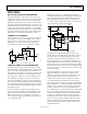
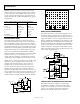


Table Of Contents
- FEATURES
- APPLICATIONS
- GENERAL DESCRIPTION
- PIN CONFIGURATIONS
- TABLE OF CONTENTS
- REVISION HISTORY
- SPECIFICATIONS
- ABSOLUTE MAXIMUM RATINGS
- TYPICAL PERFORMANCE CHARACTERISTICS
- APPLICATIONS
- RAIL-TO-RAIL APPLICATION INFORMATION
- LOW DROP-OUT REFERENCE
- LOW NOISE, SINGLE-SUPPLY PREAMPLIFIER
- DRIVING HEAVY LOADS
- DIRECT ACCESS ARRANGEMENT
- SINGLE-SUPPLY INSTRUMENTATION AMPLIFIER
- SINGLE-SUPPLY RTD THERMOMETER AMPLIFIER
- COLD JUNCTION COMPENSATED, BATTERY-POWERED THERMOCOUPLE AMPLIFIER
- 5 V ONLY, 12-BIT DAC THAT SWINGS 0 V TO 4.095 V
- 4 mA TO 20 mA CURRENT-LOOP TRANSMITTER
- 3 V LOW DROPOUT LINEAR VOLTAGE REGULATOR
- LOW DROPOUT, 500 mA VOLTAGE REGULATOR WITH FOLDBACK CURRENT LIMITING
- SQUARE WAVE OSCILLATOR
- SINGLE-SUPPLY DIFFERENTIAL SPEAKER DRIVER
- HIGH ACCURACY, SINGLE-SUPPLY, LOW POWER COMPARATOR
- OUTLINE DIMENSIONS

OP295/OP495
Rev. G | Page 11 of 16
V+
–
+
–
+
5
3
2
1
6
8
4
7
1
/
2
OP295/
OP495
1/2
OP295/
OP495
+
–
V
IN
V
O
R4
100kΩ
R3
20kΩ
R2
20kΩ
R1
100kΩ
V
REF
R
G
V
O
=
(
5+
200kΩ
)
V
IN
+V
REF
R
G
00331-022
Figure 24. Single-Supply Instrumentation Amplifier
Resistor R
G
sets the gain of the instrumentation amplifier.
Minimum gain is 6 (with no R
G
). All resistors should be matched
in absolute value as well as temperature coefficient to maximize
common-mode rejection performance and minimize drift. This
instrumentation amplifier can operate from a supply voltage as
low as 3 V.
SINGLE-SUPPLY RTD THERMOMETER AMPLIFIER
This RTD amplifier takes advantage of the rail-to-rail swing of
the OP295/OP495 to achieve a high bridge voltage in spite of a
low 5 V supply. The OP295/OP495 amplifier servos a constant
200 A current to the bridge. The return current drops across
the parallel resistors 6.19 kΩ and 2.55 M, developing a voltage
that is servoed to 1.235 V, which is established by the AD589
band gap reference. The 3-wire RTD provides an equal line
resistance drop in both 100 legs of the bridge, thus improving
the accuracy.
The AMP04 amplifies the differential bridge signal and converts
it to a single-ended output. The gain is set by the series resis-
tance of the 332 resistor plus the 50 potentiometer. The
gain scales the output to produce a 4.5 V full scale. The 0.22 F
capacitor to the output provides a 7 Hz low-pass filter to keep
noise at a minimum.
ZERO ADJ
AD589
37.4kΩ
5V
1.235
3
2
4
5
6
8
1
7
5V
AMP04
50Ω
332Ω
0.22µF
V
O
–
+
2 3
1
+–
200Ω
10-TURNS
26.7kΩ
0.5%
26.7kΩ
0.5%
100Ω
RTD
100Ω
0.5%
2
.55MΩ
1%
6.19kΩ
1%
1/2
OP295/
OP495
4.5V = 450°C
0V = 0°C
0
0331-023
Figure 25. Low Power RTD Amplifier
COLD JUNCTION COMPENSATED, BATTERY-
POWERED THERMOCOUPLE AMPLIFIER
The 150 µA quiescent current per amplifier consumption of the
OP295/OP495 makes them useful for battery-powered temperature
measuring instruments. The K-type thermocouple terminates
into an isothermal block where the terminated junctions’ ambient
temperatures can be continuously monitored and corrected by
summing an equal but opposite thermal EMF to the amplifier,
thereby canceling the error introduced by the cold junctions.
AD589
ALUMEL
CHROMEL
AL
CR
1N914
24.9kΩ
1.235
V
9V
1.33MΩ
20kΩ
2
3
4
8
–
+
–
+
–
+
1
COLD
JUNCTIONS
ISOTHERMAL
BLOCK
K-TYPE
T
HERMOCOUPLE
4
0.7µV/°
C
V
O
5V = 500°C
0V = 0°C
OP295/
OP495
SCALE
ADJUST
7.15kΩ
1%
1.5MΩ
1%
24.9kΩ
1%
475Ω
1%
2.1kΩ
1%
24.3kΩ
1%
4.99kΩ
1%
500Ω
10-TURN
ZERO
ADJUST
00331-024
Figure 26. Battery-Powered, Cold-Junction Compensated
Thermocouple Amplifier
To calibrate, immerse the thermocouple measuring junction in
a 0°C ice bath and adjust the 500 Ω zero-adjust potentiometer
to 0 V out. Then immerse the thermocouple in a 250°C tem-
perature bath or oven and adjust the scale-adjust potentiometer
for an output voltage of 2.50 V, which is equivalent to 250°C.
Within this temperature range, the K-type thermocouple is
quite accurate and produces a fairly linear transfer characteristic.
Accuracy of ±3°C is achievable without linearization.
Even if the battery voltage is allowed to decay to as low as 7 V,
the rail-to-rail swing allows temperature measurements to 700°C.
However, linearization may be necessary for temperatures above
250°C, where the thermocouple becomes rather nonlinear. The
circuit draws just under 500 A supply current from a 9 V
battery.
5 V ONLY, 12-BIT DAC THAT SWINGS 0 V TO 4.095 V
Figure 27 shows a complete voltage output DAC with wide
output voltage swing operating off a single 5 V supply. The
serial input, 12-bit DAC is configured as a voltage output device
with the 1.235 V reference feeding the current output pin (I
OUT
)
of the DAC. The V
REF
, which is normally the input, now becomes
the output.
The output voltage from the DAC is the binary weighted voltage
of the reference, which is gained up by the output amplifier such
that the DAC has a 1 mV per bit transfer function.