
Datasheet
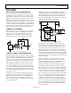
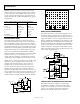


Table Of Contents
- FEATURES
- APPLICATIONS
- GENERAL DESCRIPTION
- PIN CONFIGURATIONS
- TABLE OF CONTENTS
- REVISION HISTORY
- SPECIFICATIONS
- ABSOLUTE MAXIMUM RATINGS
- TYPICAL PERFORMANCE CHARACTERISTICS
- APPLICATIONS
- RAIL-TO-RAIL APPLICATION INFORMATION
- LOW DROP-OUT REFERENCE
- LOW NOISE, SINGLE-SUPPLY PREAMPLIFIER
- DRIVING HEAVY LOADS
- DIRECT ACCESS ARRANGEMENT
- SINGLE-SUPPLY INSTRUMENTATION AMPLIFIER
- SINGLE-SUPPLY RTD THERMOMETER AMPLIFIER
- COLD JUNCTION COMPENSATED, BATTERY-POWERED THERMOCOUPLE AMPLIFIER
- 5 V ONLY, 12-BIT DAC THAT SWINGS 0 V TO 4.095 V
- 4 mA TO 20 mA CURRENT-LOOP TRANSMITTER
- 3 V LOW DROPOUT LINEAR VOLTAGE REGULATOR
- LOW DROPOUT, 500 mA VOLTAGE REGULATOR WITH FOLDBACK CURRENT LIMITING
- SQUARE WAVE OSCILLATOR
- SINGLE-SUPPLY DIFFERENTIAL SPEAKER DRIVER
- HIGH ACCURACY, SINGLE-SUPPLY, LOW POWER COMPARATOR
- OUTLINE DIMENSIONS

OP295/OP495
Rev. G | Page 12 of 16
1.23V
AD589
3
LD
2
1
3
2
4
1
8
5V
8
4765
5
V
5
V
DIGITAL
CONTROL
TOTAL POWER DISSIPATION = 1.6mW
R1
17.8kΩ
DAC8043
V
DD
R
FB
V
REF
I
OUT
GND CLK SRI
OP295/
OP495
V
O
= (4.096V)
D
4096
R4
100kΩ
R2
41.2kΩ
R3
5kΩ
+
–
0
0331-025
Figure 27. A 5 V 12-Bit DAC with 0 V to 4.095 V Output Swing
4 mA TO 20 mA CURRENT-LOOP TRANSMITTER
Figure 28 shows a self-powered 4 mA to 20 mA current-loop
transmitter. The entire circuit floats up from the single-supply
(12 V to 36 V) return. The supply current carries the signal
within the 4 mA to 20 mA range. Thus, the 4 mA establishes the
baseline current budget within which the circuit must operate.
This circuit consumes only 1.4 mA maximum quiescent
current, making 2.6 mA of current available to power additional
signal conditioning circuitry or to power a bridge circuit.
4
REF02
GND
100Ω
220Ω
2N1711
1
8
3
2
4
220pF
SPAN ADJ
NULL ADJ
HP
5082-2800
100kΩ
1%
26
5V
+
–
+
–
R
L
100Ω
12V
TO
36V
4mA
TO
20mA
100Ω
1%
1/2
OP295/
OP495
100kΩ
10-TURN
1.21MΩ
1%
182kΩ
1%
10kΩ
10-TURN
V
IN
0V + 3V
0
0331-026
Figure 28. 4 mA to 20 mA Current Loop Transmitter
3 V LOW DROPOUT LINEAR VOLTAGE REGULATOR
Figure 29 shows a simple 3 V voltage regulator design. The
regulator can deliver 50 mA load current while allowing a
0.2 V dropout voltage. The OP295/OP495 rail-to-rail output
swing drives the MJE350 pass transistor without requiring
special drive circuitry. At no load, its output can swing less than
the pass transistor’s base-emitter voltage, turning the device
nearly off. At full load, and at low emitter-collector voltages, the
transistor beta tends to decrease. The additional base current is
easily handled by the OP295/OP495 output.
The amplifier servos the output to a constant voltage, which
feeds a portion of the signal to the error amplifier.
Higher output current, to 100 mA, is achievable at a higher
dropout voltage of 3.8 V.
V
IN
5V TO 3.2V
MJE 350
43kΩ
AD589
1.235V
3
2
4
1
8
1000pF
I
L
< 50m
A
V
O
100µF
44.2kΩ
1%
30.9kΩ
1%
1/2
OP295/
OP495
+
–
0
0331-027
+
+
Figure 29. 3 V Low Dropout Voltage Regulator
Figure 30 shows the regulator’s recovery characteristic when its
output underwent a 20 mA to 50 mA step current change.
10
100
0%
90
1ms20mV
2V
50mA
20mA
OUTPUT
STEP
CURRENT
CONTROL
W
AVEFORM
00331-028
Figure 30. Output Step Load Current Recovery
LOW DROPOUT, 500 mA VOLTAGE REGULATOR
WITH FOLDBACK CURRENT LIMITING
Adding a second amplifier in the regulation loop, as shown in
Figure 31, provides an output current monitor as well as
foldback current limiting protection.
IRF9531
G
6V
REF43
2
4
6
2.5V
A2
A1
1
4
2
3
5
6
7
8
1N4148
I
O
(NORM) = 0.5
A
I
O
(MAX) = 1A
RSENSE
0.1Ω
1/4W
SD
5V V
O
+
–
1/2
OP295/
OP495
1/2
OP295/
OP495
0.01µF
100kΩ
5%
205kΩ
1%
210kΩ
1%
45.3kΩ
1%
45.3kΩ
1%
124kΩ
1%
124kΩ
1%
00331-029
+
–
+
–
Figure 31. Low Dropout, 500 mA Voltage Regulator
with Foldback Current Limiting