
Datasheet
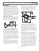


Table Of Contents
- FEATURES
- APPLICATIONS
- GENERAL DESCRIPTION
- PIN CONFIGURATIONS
- TABLE OF CONTENTS
- REVISION HISTORY
- SPECIFICATIONS
- ABSOLUTE MAXIMUM RATINGS
- TYPICAL PERFORMANCE CHARACTERISTICS
- APPLICATIONS
- RAIL-TO-RAIL APPLICATION INFORMATION
- LOW DROP-OUT REFERENCE
- LOW NOISE, SINGLE-SUPPLY PREAMPLIFIER
- DRIVING HEAVY LOADS
- DIRECT ACCESS ARRANGEMENT
- SINGLE-SUPPLY INSTRUMENTATION AMPLIFIER
- SINGLE-SUPPLY RTD THERMOMETER AMPLIFIER
- COLD JUNCTION COMPENSATED, BATTERY-POWERED THERMOCOUPLE AMPLIFIER
- 5 V ONLY, 12-BIT DAC THAT SWINGS 0 V TO 4.095 V
- 4 mA TO 20 mA CURRENT-LOOP TRANSMITTER
- 3 V LOW DROPOUT LINEAR VOLTAGE REGULATOR
- LOW DROPOUT, 500 mA VOLTAGE REGULATOR WITH FOLDBACK CURRENT LIMITING
- SQUARE WAVE OSCILLATOR
- SINGLE-SUPPLY DIFFERENTIAL SPEAKER DRIVER
- HIGH ACCURACY, SINGLE-SUPPLY, LOW POWER COMPARATOR
- OUTLINE DIMENSIONS

OP295/OP495
Rev. G | Page 13 of 16
V
+
100kΩ
100kΩ
58.7kΩ
R
FREQ OUT
4
1
8
3
2
C
1
RC
F
OSC
= < 350Hz @ V+ = 5V
1/2
OP295/
OP495
+
–
+
00331-030
Amplifier A1 provides error amplification for the normal
voltage regulation loop. As long as the output current is less
than 1 A, the output of Amplifier A2 swings to ground, reverse-
biasing the diode and effectively taking itself out of the circuit.
However, as the output current exceeds 1 A, the voltage that
develops across the 0.1 sense resistor forces the output of
Amplifier A2 to go high, forward-biasing the diode, which in
turn closes the current-limit loop. At this point, the A2’s lower
output resistance dominates the drive to the power MOSFET
transistor, thereby effectively removing the A1 voltage regula-
tion loop from the circuit.
Figure 32. Square Wave Oscillator Has Stable Frequency Regardless of
Supply Changes
If the output current greater than 1 A persists, the current limit
loop forces a reduction of current to the load, which causes a
corresponding drop in output voltage. As the output voltage
drops, the current-limit threshold also drops fractionally,
resulting in a decreasing output current as the output voltage
decreases, to the limit of less than 0.2 A at 1 V output. This fold-
back effect reduces the power dissipation considerably during a
short circuit condition, thus making the power supply far more
forgiving in terms of the thermal design requirements. Small
heat sinking on the power MOSFET can be tolerated.
10kΩ
90.9kΩ
V+
100kΩ
10kΩ
20kΩ 20kΩ
V+
SPEAKER
+
+
1/4
OP295/
OP495
1/4
OP295/
OP495
1/4
OP295/
OP495
V
IN
2.2µF
–
+
–
+
–
+
00331-031
The rail-to-rail swing of the OP295 exacts higher gate drive to
the power MOSFET, providing a fuller enhancement to the tran-
sistor. The regulator exhibits 0.2 V dropout at 500 mA of load
current. At 1 A output, the dropout voltage is typically 5.6 V.
Figure 33. Single-Supply Differential Speaker Driver
HIGH ACCURACY, SINGLE-SUPPLY, LOW POWER
COMPARATOR
SQUARE WAVE OSCILLATOR
The OP295/OP495 make accurate open-loop comparators.
With a single 5 V supply, the offset error is less than 300 V.
Figure 34 shows the response time of the OP295/OP495 when
operating open-loop with 4 mV overdrive. They exhibit a 4 ms
response time at the rising edge and a 1.5 ms response time at
the falling edge.
The circuit in Figure 32 is a square wave oscillator (note the
positive feedback). The rail-to-rail swing of the OP295/OP495
helps maintain a constant oscillation frequency even if the supply
voltage varies considerably. Consider a battery-powered system
where the voltages are not regulated and drop over time. The
rail-to-rail swing ensures that the noninverting input sees the
full V+/2, rather than only a fraction of it.
10
100
0%
90
5ms
2V
1V
OUTPUT
INPUT
(5mV OVERDRIVE
@ OP295 INPUT)
00331-032
The constant frequency comes from the fact that the 58.7 k
feedback sets up Schmitt trigger threshold levels that are directly
proportional to the supply voltage, as are the RC charge voltage
levels. As a result, the RC charge time, and therefore, the frequency,
remain constant, independent of supply voltage. The slew rate
of the amplifier limits oscillation frequency to a maximum of about
800 Hz at a 5 V supply.
SINGLE-SUPPLY DIFFERENTIAL SPEAKER DRIVER
Connected as a differential speaker driver, the OP295/OP495
can deliver a minimum of 10 mA to the load. With a 600 load,
the OP295/OP495 can swing close to 5 V p-p across the load.
Figure 34. Open-Loop Comparator Response Time with 5 mV Overdrive