
Datasheet
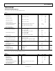
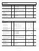
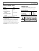
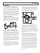
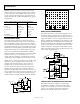
Table Of Contents
- FEATURES
- APPLICATIONS
- GENERAL DESCRIPTION
- PIN CONFIGURATIONS
- TABLE OF CONTENTS
- REVISION HISTORY
- SPECIFICATIONS
- ABSOLUTE MAXIMUM RATINGS
- TYPICAL PERFORMANCE CHARACTERISTICS
- APPLICATIONS
- RAIL-TO-RAIL APPLICATION INFORMATION
- LOW DROP-OUT REFERENCE
- LOW NOISE, SINGLE-SUPPLY PREAMPLIFIER
- DRIVING HEAVY LOADS
- DIRECT ACCESS ARRANGEMENT
- SINGLE-SUPPLY INSTRUMENTATION AMPLIFIER
- SINGLE-SUPPLY RTD THERMOMETER AMPLIFIER
- COLD JUNCTION COMPENSATED, BATTERY-POWERED THERMOCOUPLE AMPLIFIER
- 5 V ONLY, 12-BIT DAC THAT SWINGS 0 V TO 4.095 V
- 4 mA TO 20 mA CURRENT-LOOP TRANSMITTER
- 3 V LOW DROPOUT LINEAR VOLTAGE REGULATOR
- LOW DROPOUT, 500 mA VOLTAGE REGULATOR WITH FOLDBACK CURRENT LIMITING
- SQUARE WAVE OSCILLATOR
- SINGLE-SUPPLY DIFFERENTIAL SPEAKER DRIVER
- HIGH ACCURACY, SINGLE-SUPPLY, LOW POWER COMPARATOR
- OUTLINE DIMENSIONS

OP295/OP495
Rev. G | Page 2 of 16
TABLE OF CONTENTS
Features .............................................................................................. 1
Applications ....................................................................................... 1
General Description ......................................................................... 1
Pin Configurations ........................................................................... 1
Revision History ............................................................................... 2
Specifications ..................................................................................... 3
Electrical Characteristics ............................................................. 3
Absolute Maximum Ratings ............................................................ 5
Thermal Resistance ...................................................................... 5
ESD Caution .................................................................................. 5
Typical Performance Characteristics ............................................. 6
Applications ....................................................................................... 9
Rail-to-Rail Application Information ........................................ 9
Low Drop-Out Reference ............................................................ 9
Low Noise, Single-Supply Preamplifier ..................................... 9
Driving Heavy Loads ................................................................. 10
Direct Access Arrangement ...................................................... 10
Single-Supply Instrumentation Amplifier .............................. 10
Single-Supply RTD Thermometer Amplifier ......................... 11
Cold Junction Compensated, Battery-Powered
Thermocouple Amplifier .......................................................... 11
5 V Only, 12-Bit DAC That Swings 0 V to 4.095 V .................... 11
4 mA to 20 mA Current-Loop Transmitter ............................ 12
3 V Low Dropout Linear Voltage Regulator ............................. 12
Low Dropout, 500 mA Voltage Regulator with Foldback
Current Limiting ........................................................................ 12
Square Wave Oscillator .............................................................. 13
Single-Supply Differential Speaker Driver .............................. 13
High Accuracy, Single-Supply, Low Power Comparator ...... 13
Outline Dimensions ....................................................................... 14
Ordering Guide .......................................................................... 16
REVISION HISTORY
8/09—Rev. F to Rev. G
Added Figure 18 ................................................................................ 8
Updated Outline Dimensions ....................................................... 17
3/08—Rev. E to Rev. F
Changes to Offset Voltage Unit in Table 1 .................................... 3
Updated Outline Dimensions ....................................................... 14
Changes to Ordering Guide .......................................................... 16
5/06—Rev. D to Rev. E
Updated Format .................................................................. Universal
Changes to Features .......................................................................... 1
Changes to Pin Connections ........................................................... 1
Updated Outline Dimensions ....................................................... 14
Changes to Ordering Guide .......................................................... 15
2/04—Rev. C to Rev. D
Changes to General Description .................................................... 1
Changes to Specifications ................................................................ 2
Changes to Absolute Maximum Ratings ....................................... 4
Changes to Ordering Guide ............................................................ 4
Updated Outline Dimensions ....................................................... 12
3/02—Rev. B to Rev. C
Figure changes to Pin Connections ................................................ 1
Deleted OP295GBC and OP495GBC from Ordering Guide ...... 3
Deleted Wafer Test Limits Table ...................................................... 3
Changes to Absolute Maximum Ratings ........................................ 4
Deleted Dice Characteristics ............................................................ 4