
Datasheet
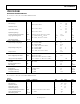
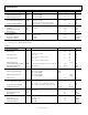
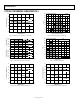
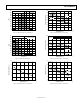
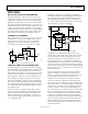
Table Of Contents
- FEATURES
- APPLICATIONS
- GENERAL DESCRIPTION
- PIN CONFIGURATIONS
- TABLE OF CONTENTS
- REVISION HISTORY
- SPECIFICATIONS
- ABSOLUTE MAXIMUM RATINGS
- TYPICAL PERFORMANCE CHARACTERISTICS
- APPLICATIONS
- RAIL-TO-RAIL APPLICATION INFORMATION
- LOW DROP-OUT REFERENCE
- LOW NOISE, SINGLE-SUPPLY PREAMPLIFIER
- DRIVING HEAVY LOADS
- DIRECT ACCESS ARRANGEMENT
- SINGLE-SUPPLY INSTRUMENTATION AMPLIFIER
- SINGLE-SUPPLY RTD THERMOMETER AMPLIFIER
- COLD JUNCTION COMPENSATED, BATTERY-POWERED THERMOCOUPLE AMPLIFIER
- 5 V ONLY, 12-BIT DAC THAT SWINGS 0 V TO 4.095 V
- 4 mA TO 20 mA CURRENT-LOOP TRANSMITTER
- 3 V LOW DROPOUT LINEAR VOLTAGE REGULATOR
- LOW DROPOUT, 500 mA VOLTAGE REGULATOR WITH FOLDBACK CURRENT LIMITING
- SQUARE WAVE OSCILLATOR
- SINGLE-SUPPLY DIFFERENTIAL SPEAKER DRIVER
- HIGH ACCURACY, SINGLE-SUPPLY, LOW POWER COMPARATOR
- OUTLINE DIMENSIONS

OP295/OP495
Rev. G | Page 5 of 16
ABSOLUTE MAXIMUM RATINGS
THERMAL RESISTANCE
Table 4.
Parameter
1
Rating
Supply Voltage ±18 V
Input Voltage ±18 V
Differential Input Voltage
2
36 V
Output Short-Circuit Duration Indefinite
Storage Temperature Range
P, S Packages −65°C to +150°C
Operating Temperature Range
OP295G, OP495G –40°C to +125°C
Junction Temperature Range
P, S Packages –65°C to +150°C
Lead Temperature (Soldering, 60 sec) 300°C
θ
JA
is specified for worst case mounting conditions; that is, θ
JA
is specified for device in socket for PDIP; θ
JA
is specified for
device soldered to printed circuit board for SOIC package.
Table 5. Thermal Resistance
Package Type θ
JA
θ
JC
Unit
8-Lead PDIP (N-8) 103 43 °C/W
8-Lead SOIC_N (R-8) 158 43 °C/W
14-Lead PDIP (N-14) 83 39 °C/W
16-Lead SOIC_W (RW-16) 98 30 °C/W
ESD CAUTION
1
Absolute maximum ratings apply to packaged parts, unless otherwise noted.
2
For supply voltages less than ±18 V, the absolute maximum input voltage is
equal to the supply voltage.
Stresses above those listed under Absolute Maximum Ratings
may cause permanent damage to the device. This is a stress
rating only; functional operation of the device at these or any
other conditions above those indicated in the operational
section of this specification is not implied. Exposure to absolute
maximum rating conditions for extended periods may affect
device reliability.