
Datasheet


REV.
OP777/OP727/OP747
–10–
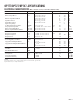
TEMPERATURE – C
OUTPUT VOLTAGE HIGH – V
14.944
60
40
140
20
0
20 40 60 80 100 120
14.946
14.948
14.950
14.954
14.956
14.958
14.960
14.962
14.964
V
SY
= 15V
I
L
= 1mA
14.952
TPC 46. Output Voltage High vs.
Temperature
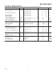
TEMPERATURE – C
OUTPUT VOLTAGE LOW – V
14.960
60
40
140
V
SY
= 15V
I
L
= 1mA
20
0
20 40 60 80 100 120
14.955
14.950
14.945
14.935
14.930
14.940
TPC 47. Output Voltage Low vs.
Temperature
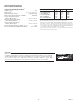
TIME – Minutes
V
OS
– V
1.5
0
1.5
0
0.5 5.0
1.0 1.5 2.0 2.5 3.0 3.5 4.0 4.5
1.0
0.5
0.5
1.0
V
SY
= 15V
V
CM
= 0V
T
A
= 25C
TPC 48. Warm-Up Drift
BASIC OPERATION
The OP777/OP727/OP747 amplifier uses a precision Bipolar
PNP input stage coupled with a high-voltage CMOS output
stage. This enables this amplifier to feature an input voltage
range which includes the negative supply voltage (often ground-
in single-supply applications) and also swing to within 1 mV of the
output rails. Additionally, the input voltage range extends to within
1 V of the positive supply rail. The epitaxial PNP input structure
provides high breakdown voltage, high gain, and an input bias cur-
rent figure comparable to that obtained with a “Darlington” input
stage amplifier but without the drawbacks (i.e., severe penalties for
input voltage range, offset, drift and noise). The PNP input structure
also greatly lowers the noise and reduces the dc input error terms.
Supply Voltage
The amplifiers are fully specified with a single 5 V supply and, due
to design and process innovations, can also operate with a supply
voltage from V up to 30 V. This allows operation from most
split supplies used in current industry practice, with the advantage
of substantially increased input and output voltage ranges over
conventional split-supply amplifiers. The OP777/OP727/OP747
series is specified with (V
SY
= 5 V, V– = 0 V and V
CM
= 2.5 V
which is most suitable for single-supply application. With PSRR of
130 dB (0.3 μV/V) and CMRR of 110 dB (3 μV/V) offset is mini-
mally affected by power supply or common-mode voltages. Dual
supply, ±15 V operation is also fully specified.
Input Common-Mode Voltage Range
The OP777/OP727/OP747 is rated with an input common-mode
voltage which extends from the minus supply to within 1 V of the
positive supply. However, the amplifier can still operate with input
voltages slightly below V
EE
. In Figure 2, OP777/OP727/OP747 is
configured as a difference amplifier with a single supply of V
and negative dc common-mode voltages applied at the inputs
terminals. A 400 mV p-p input is then applied to the noninverting
input. It can be seen from the graph below that the output does not
show any distortion. Micropower operation is maintained by using
large input and feedback resistors.
Figure 1. Input and Output Signals with V
CM
< 0 V
+3V
OP777/
OP727/
OP747
100k
100k
100k
100k
0.1V
V
IN
= 1kHz at 400mV p-p
0.27V
Figure 2. OP777/OP727/OP747 Configured as a Differ-
ence Amplifier Operating at V
CM
< 0 V
D
3.0
3.0
TIME – 0.2ms/DIV
V
IN
0V
V
OUT
VOLTAGE – 100mV/DIV