
Datasheet


10 V Precision
Voltage Reference
REF01
Rev. H
Information furnished by Analog Devices is believed to be accurate and reliable. However, no
responsibility is assumed by Analog Devices for its use, nor for any infringements of patents or other
rights of third parties that may result from its use. Specifications subject to change without notice. No
license is granted by implication or otherwise under any patent or patent rights of Analog Devices.
Trademarks and registered trademarks are the property of their respective owners.
One Technology Way, P.O. Box 9106, Norwood, MA 02062-9106, U.S.A.
Tel: 781.329.4700
www.analog.com
Fax: 781.461.3113 © 2005 Analog Devices, Inc. All rights reserved.
FEATURES
10 V output, ±0.3% maximum
Adjustment range, ±3% minimum
Excellent temperature stability, 8.5 ppm/°C maximum
Low noise, 30 µV p-p maximum
Low supply current, 1.4 mA maximum
Wide input voltage range, 12 V to 40 V
High load driving capability, 10 mA
No external components
Short-circuit proof
GENERAL DESCRIPTION
The REF01 precision voltage reference provides a stable 10 V
output that can be adjusted over a 3% range with minimal effect
on temperature stability. Single-supply operation over an input
voltage range of 12 V to 40 V, a low current drain of 1 mA, and
excellent temperature stability are achieved with an improved
band gap design. Low cost, low noise, and low power make the
REF01 an excellent choice whenever a stable voltage reference is
required. Applications include DACs and ADCs, portable
instrumentation, and digital voltmeters. Full military
temperature range devices with screening to MIL-STD-883 are
available. For new designs, refer to ADR01.
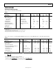
PIN CONFIGURATIONS
00373-F-001
1
2
3
4
5
6
7
8
NC
GROUND
(CASE)
NC
V
IN
V
OUT
NC
NC TRIM
NC = NO CONNECT. DO NOT CONNECT ANYTHING
ON THESE PINS. SOME OF THEM ARE RESERVED
FOR FACTORY TESTING PURPOSES.
Figure 1. TO-99 (J Suffix)
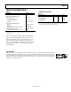
00373-F-002
REF01
TOP VIEW
(Not to Scale)
NC
1
V
IN
2
NC
3
GND
4
NC
NC
V
OUT
TRIM
8
7
6
5
NC = NO CONNECT. DO NOT CONNECT ANYTHING
ON THESE PINS. SOME OF THEM ARE RESERVED
FOR FACTORY TESTING PURPOSES.
Figure 2. 8-Lead PDIP (P-Suffix)
8-Lead CERDIP (Z-Suffix)
8-Lead SOIC (S-Suffix)
00373-F-003
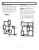
REF01 OPTION R9 R11 R12
P AND S PACKAGES 18kΩ 4.5kΩ 33.3kΩ
J AND Z PACKAGES, 50kΩ 2kΩ 16.7kΩ
AND 883C PRODUCT
OUTPUT RESISTORS
C1
R3
R6
R4
R5
R1
Q1
R2
R10
OUTPUT
GROUND
R12*
TRIM
Q19
R15
INPUT
Q15
Q18
Q16
Q13
Q21
Q17
R13
Q20
Q4
Q3
Q5
Q6
Q9
Q7
Q14
Q12
Q11
Q8
R8
R7
R14
Q10
Q2
R11*
R9*
4
5
6
≈1.23V
2
*SEE OUTPUT RESISTORS
Figure 3. Simplified Schematic