
Datasheet


REF01
Rev. H | Page 10 of 12
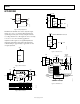
PRECISION CURRENT SOURCE
A current source with 25 V output compliance and excellent
output impedance can be obtained using this circuit. REF01
keeps the line voltage and power dissipation constant in the
device; the only important error consideration at room
temperature is the negative supply rejection of the op amp.
The typical 3 µV/V PSRR of the OP02E creates an 8 ppm
change (3 µV/V × 25 V/10 V) in output current over a 25 V
range. For example, a 10 mA current source can be built
(R = 1 kΩ) with 300 MΩ output impedance.
mA10108
V25
6
××
=
−
O
R
00373-F-020
GND
REF01
GND
REF01
OP02E
C
C
R
2
2
2
6
6
7
3
4
6
4
4
+50V
–5V
I
O
=
10V
R
RC = 10
–5
SEC
R
(TRIM FOR
CALIBRATION)
V
IN
V
O
V
IN
V
O
V
O
= 0V
TO 25V
1
2
Figure 20. Precision Current Source
SUPPLY BYPASSING
For best results, it is recommended that the power supply pin be
bypassed with a 0.1 µF disc ceramic capacitor.
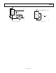
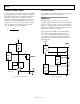
REFERENCE STACK WITH EXCELLENT LINE
REGULATION
Three REF01s can be stacked to yield 10 V, 20 V, and 30 V
outputs. An additional advantage is near-perfect line regulation
of the 10.0 V and 20.0 V output. A 32 V to 60 V input change
produces an output change that is less than the noise voltage of
the devices. A load bypass resistor (R
B
) provides a path for the
supply current (I
SY
) of the 20 V regulator.
In general, any number of REF01s can be stacked this way.
For example, 10 devices will yield outputs of 10 V, 20 V,
30 V . . . 100 V. The line voltage can change from 105 V to
130 V. However, care must be taken to ensure that the total
load currents do not exceed the maximum usable current
(typically 21 mA).
00373-F-021
GND
REF01
GND
REF01
GND
REF01
TRIM
TRIM
10kΩ
10kΩ
R
B
6.8kΩ
10kΩ
2
6
5
4
2
6
5
4
2
6
5
4
30V
20V
10V
TRIM
32V TO 60V
TRIMMED
OUTPUTS
V
IN
V
O
V
IN
V
O
V
IN
V
O
Figure 21. Reference Stack