
Datasheet


REF01
Rev. H | Page 4 of 12
@ V
IN
= 15 V, T
A
= 25°C, unless otherwise noted.
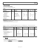
Table 3.
REF01C
Parameter Symbol Conditions Min Typ Max Unit
Output Voltage V
O
I
L
= 0 mA 9.90 10.00 10.10 V
Output Adjustment Range ∆V
TRIM
R
P
= 10 kΩ ±2.7 ±3.3 %
Output Voltage Noise
1
S, Z, P Packages
J, 883 Parts
e
n p-p
e
n p-p
0.1 Hz to 10 Hz
0.1 Hz to 10 Hz
30
35
µV p-p
µV p-p
Line Regulation
2
V
IN
= 13 V to 33 V 0.009 0.015 %/V
Load Regulation
2
I
L
= 0 mA to 8 mA 0.006 0.015 %/mA
Turn-On Settling Time
3
t
ON
To ±0.1% of final value 5 µs
Quiescent Supply Current I
SY
No load 1.0 1.6 mA
Load Current I
L
8 mA
Sink Current
4
I
S
−0.3 −0.5 mA
Short-Circuit Current I
SC
V
O
= 0 30 mA
1
Sample tested.
2
Line and load regulation specifications include the effect of self-heating.
3
Guaranteed by design, not production tested.
4
During sink current test, the device meets the output voltage specified.
@ V
IN
= 15 V, 0°C ≤ T
A
≤ +70°C for REF01CJ, REF01CZ, and −40°C ≤ T
A
≤ +85°C for REF01CP and REF01CS, unless otherwise noted.
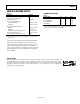
Table 4.
REF01C
Parameter Symbol Conditions Min Typ Max Unit
Output Voltage Change ∆V
OT
0.14 0.45 %
with Temperature
1, 2
Output Voltage TCV
O
20 65 ppm/°C
Temperature Coefficient
3
Change in V
O
Temperature
Coefficient with Output
Adjustment R
P
= 10 kΩ 0.7 ppm/°C
Line Regulation
4
V
IN
=13 V to 30 V 0.011 0.018 %/V
Load Regulation
4
I
L
= 0 to 5 mV 0.008 0.018 %/mA
1
∆V
OT
is defined as the absolute difference between the maximum output voltage and the minimum output voltage over the specified temperature range expressed as
a percentage of 10 V:
100
10
×
−
=∆
V
VV
V
MINMAX
OT
2
∆V
OT
specification applies trimmed to +10,000 V or untrimmed.
3
TCV
O
is defined as ∆Var divided by the temperature range; therefore,
()
()
C70
C70C0
C70C0
°
°+°∆
=°+°
toV
toTCV
OT
O
and
()
()
C180
C125C55
C125C55
°
°+°−∆
=°+°−
toV
toTCV
OT
O
4
Line and load regulation specifications include the effect of self-heating.