
Datasheet


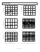
Table Of Contents

Precision 2.5 V, 5.0 V, and 10.0 V
Voltage References
Data Sheet
REF01/REF02/REF03
Rev. M Document Feedback
Information f
urnished by Analog Devices is believed to be accurate and reliable. However, no
responsibility is assumed by Analog Devices for its use, nor for any infringements of patents or other
rights of third parties that may result from its use. Specifications subject to change without notice. No
license is granted by implication or otherwise under any patent or patent rights of Analog Devices.
Trademarks and registered trademarks are the property of their respective owners.
One Technology Way, P.O. Box 9106, Norwood, MA 02062-9106, U.S.A.
Tel: 781.329.4700 ©2009–2016 Analog Devices, Inc. All rights reserved.
Technical Support www.analog.com
FEATURES
High output accuracy
REF01: 10.0 V, ±0.3% maximum
REF02: 5.0 V, ±0.3% maximum
REF03: 2.5 V, ±0.6% maximum
Adjustable output: ± 3% minimum
Excellent temperature stability
REF01: 8.5 ppm/°C maximum
REF02: 8.5 ppm/°C maximum
REF03: 50 ppm/°C maximum
Low noise
REF01: 30 µV p-p typical
REF02: 15 µV p-p typical
REF03: 6 µV p-p typical
High supply voltage range: up to 36 V maximum
Low supply current: 1.4 mA maximum
High load-driving capability: 10 mA maximum
Temperature output function
APPLICATIONS
Precision data systems
High resolution converters
Industrial process control systems
Precision instruments
Military and aerospace applications
GENERAL DESCRIPTION
The REF01/REF02/REF03 series of precision voltage references
provide a stable 10.0 V, 5.0 V, or 2.5 V output with minimal change
in response to variations in supply voltage, ambient temperature
or load conditions. The devices are available in 8-lead SOIC, PDIP,
CERDIP, and TO-99 packages, as well as 20-terminal LCC
packages (883 only), furthering the usability of the devices in
both standard and high stress applications.
With an external buffer and a simple resistor network, the
TEMP terminal can be used for temperature sensing and
approximation. A TRIM terminal is also provided on the
device for fine adjustment of the output voltage.
The small footprint, wide supply range, and application
versatility make the REF01/REF02/REF03 series of references
ideal for general-purpose and space-constrained applications.
Newer designs should use the ADR01/ADR02/ADR03/ADR06
series of references, which offer higher accuracy and temperature
PIN CONFIGURATIONS
00375-001
REF01/
REF02/
REF03
TO
P VIEW
(Not to Scale)
NC
1
V
IN
2
TEM
P
3
GND
4
NC
NC
V
OUT
TRIM
8
7
6
5
NC = NO CONNEC
T. DO NOT CONNECT ANYTHING
ON THESE PINS. SOME OF THEMARE RESE
RVED
FOR
FAC
T
OR
Y
TESTING PURPOSES.
Figure 1. 8-Lead PDIP (P-Suffix),
8-Lead CERDIP (Z-Suffix),
8-Lead SOIC (S-Suffix)
00375-002
1
2
3
4
5
6
7
8
NC
GROUND
(CASE)
NC
V
IN
V
OUT
NC
NC TRIM
NC = NO CONNECT. DO NOT CONNECT
ANYTHING
ON THESE PINS. SOME OF THEMARE RESERVED
FOR FACTORY TESTING PURPOSES.
REF01/
REF02/
REF03
Figure 2. 8-Lead TO-99 (J-Suffix)
00375-003
4
NC
5
V
IN
6
NC
7
TEMP
8
NC
18
NC
17
NC
16
NC
15
V
OUT
14
NC
19
NC
20
NC
1
NC
2
NC
3
NC
13
NC
12
TRIM
11
NC
10
GND
9
NC
REF01/
REF02
TOP VIEW
(Not to Scale)
NC = NO CONNECT. DO NOT CONNECT ANYTHING
ON THESE PINS. SOME OF THEMARE RESERVED
FOR FACTORY TESTING PURPOSES.
Figure 3. 20-Terminal LCC (RC-Suffix;
883 Devices Only)
stability over a wider operating temperature range, while maintain-
ing full pin-for-pin compatibility with the REF01/REF02/REF03
series. This data sheet applies to commercial-grade products
only. Contact sales or visit analog.com for military-grade (883)
data sheets.
Table 1. Selection Guide
Device Number Output Voltage Input Voltage Range
REF01
10.0 V
12 V to 36 V
REF02 5.0 V 7.0 V to 36 V
REF03 2.5 V 4.5 V to 36 V