
Datasheet
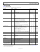
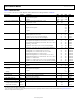

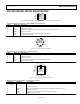
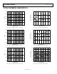

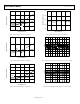
Table Of Contents

Data Sheet REF01/REF02/REF03
Rev. M | Page 7 of 20
PIN CONFIGURATIONS AND FUNCTION DESCRIPTIONS
00375-004
REF01/
REF02/
REF03
T
OP
VIEW
(Not to Scale)
NC
1
V
IN
2
TEMP
3
GND
4
NC
NC
V
OUT
TRIM
8
7
6
5
Figure 4.
8-Lead PDIP (P-Suffix), 8-Lead CERDIP (Z-Suffix), 8-Lead SOIC (S-Suffix) Pin Configuration
Table 4. Pin Function Descriptions—PDIP, CERDIP, and SOIC Packages
Pin No. Mnemonic Description
1, 7, 8 NC No Internal Connection. Leave floating or tied to ground in actual application.
2 V
IN
Supply Voltage Input.
3 TEMP Temperature (Band Gap) Output. Refer to the Temperature Monitoring section.
4
GND
Ground Connection.
5 TRIM Output Voltage Trim. Refer to the Output Adjustment section.
6 V
OUT
Reference Voltage Output.
00375-005
1
2
3
4
5
6
7
8
NC
GROUND
(CASE)
NC
V
IN
V
OUT
NC
NC TRIM
REF01/
REF02/
REF03
Figure 5. 8-Lead TO-99 (J-Suffix) Pin Configuration
Table 5. Pin Function Descriptions—8-Lead TO-99 Package
Pin No. Mnemonic Description
1, 3, 7, 8 NC No Internal Connection. Leave floating or tied to ground in actual application.
2 V
IN
Supply Voltage Input.
4 GND Ground Connection.
5 TRIM Output Voltage Trim. Refer to the Output Adjustment section.
6 V
OUT
Reference Voltage Output.
00375-006
4
NC
5
V
IN
6
NC
7
TEMP
8
NC
18
NC
17
NC
16
NC
15
V
OUT
14
NC
19
NC
20
NC
1
NC
2
NC
3
NC
13
NC
12
TRIM
1
1
NC
10
GND
9
NC
REF01/
REF02
TO
P VIEW
(Not to Scale)
Figure 6.
20-Terminal LCC (RC-Suffix) Pin Configuration
Table 6. Pin Function Descriptions—20-Terminal LCC Package
Terminal No. Mnemonic Description
1 to4, 6, 8, 9, 11,
13, 14, 16 to 20
NC No Internal Connection. Leave floating or tied to ground in actual application.
5 V
IN
Supply Voltage Input.
7 TEMP Temperature (Band Gap) Output. Refer to the Temperature Monitoring section.
10 GND Ground Connection.
12 TRIM Output Voltage Trim. Refer to the Output Adjustment section.
15 V
OUT
Reference Voltage Output.