
Datasheet

Data Sheet REF19x Series
Rev. L | Page 5 of 28
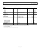
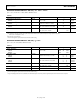
ELECTRICAL CHARACTERISTICS—REF191 @ −40°C ≤ +85°C
@ V
S
= 3.3 V, −40°C ≤ T
A
≤ +85°C, unless otherwise noted.
Table 3.
Parameter Symbol Condition Min Typ Max Unit
TEMPERATURE COEFFICIENT
1, 2
TCV
O
/°C
E Grade I
OUT
= 0 mA 2 5 ppm/°C
F Grade 5 10 ppm/°C
G Grade
3
10 25 ppm/°C
LINE REGULATION
4
ΔV
O
/ΔV
IN
E Grade 3.0 V ≤ V
S
≤ 15 V, I
OUT
= 0 mA 5 10 ppm/V
F and G Grades 10 20 ppm/V
LOAD REGULATION
4
ΔV
O
/ΔV
LOAD
E Grade V
S
= 5.0 V, 0 mA ≤ I
OUT
≤ 25 mA 5 15 ppm/mA
F and G Grades 10 20 ppm/mA
DROPOUT VOLTAGE V
S
− V
O
V
S
= 3.0 V, I
LOAD
= 2 mA 0.95 V
V
S
= 3.3 V, I
LOAD
= 10 mA 1.25 V
V
S
= 3.6 V, I
LOAD
= 25 mA 1.55 V
SLEEP
PIN
Logic High Input Voltage V
H
2.4 V
Logic High Input Current I
H
−8 μA
Logic Low Input Voltage V
L
0.8 V
Logic Low Input Current I
L
−8 μA
SUPPLY CURRENT No load 45 μA
Sleep Mode No load 15 μA
1
For proper operation, a 1 μF capacitor is required between the output pin and the GND pin of the device.
2
TCV
O
is defined as the ratio of output change with temperature variation to the specified temperature range expressed in ppm/°C.
TCV
O
= (V
MAX
− V
MIN
)/V
O
(T
MAX
− T
MIN
)
3
Guaranteed by characterization.
4
Line and load regulation specifications include the effect of self-heating.