
Inc. SHARC EZ-Extender Manual


SHARC EZ-Extender Manual 2-3
EZ-Extender Hardware Reference
ing a socket with an oscillator. Only one of these sources can be used at a
time, the other sources must be disabled. For more information on how to
disable the TX_CLK sources, see “SMA Connector Clock Disconnect
Jumper (P10)” on page 2-5. The RX_CLK signal is generated by the target
board. Both the TX_CLK and RX_CLK can connect to the processor’s clock-in
signal (DAI_P2_CLOCKIN) as an input. See “Direction/Clock Source Con-
trol Switch (SW1)” on page 2-3 for more information.
The ADC interface has two general-purpose signals, DAI_P15_GP1 and
DAI_P16_GP2. The evaluation board with which the extender interfaces
determines how these signals are set up. For information on how to set the
direction and the source of these signals, refer to “Direction/Clock Source
Control Switch (SW1)” on page 2-3.
The ADC interface connects to the PDAP of the ADSP-21262 processor.
The PDAP is multiplexed with the address and data bus. To avoid bus
contention with the memory devices on the EZ-KIT Lite, the driver con-
nected to the data bus of the ADC must be enabled. For more information
about enabling the data bus, see “ADC HSC Interface” on page 1-1.
DIP Switches and Jumpers
The following section describes the function of all of the jumpers and
switches on the EZ-Extender. Before connecting the extender, familiarize
yourself with each possible setting’s effect on your application.
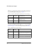
Direction/Clock Source Control Switch (SW1)
A designated DIP switch, SW1, provides an independent direction control
for the general-purpose signals (DAI_P15_GP1 and DAI_P16_GP2), as illus-
trated in Figure 2-1 on page 2-2. Each signal can be hardwired to be either
transmit or receive, or can be changed in real time using the DAI_P18 pro-
cessor pin. If the DAI_P18 processor pin is intended for the direction
control, ensure the pin is not used for other purposes on the EZ-KIT Lite.