TigerSHARC® Embedded Processor ADSP-TS201S • a KEY FEATURES KEY BENEFITS Up to 600 MHz, 1.
ADSP-TS201S TABLE OF CONTENTS General Description ................................................. 3 Test Conditions .................................................. 37 Dual Compute Blocks ............................................ 4 Output Disable Time ......................................... 37 Data Alignment Buffer (DAB) .................................. 4 Output Enable Time ......................................... 38 Dual Integer ALU (IALU) .......................................
ADSP-TS201S GENERAL DESCRIPTION The ADSP-TS201S TigerSHARC processor is an ultrahigh performance, static superscalar processor optimized for large signal processing tasks and communications infrastructure. The DSP combines very wide memory widths with dual computation blocks—supporting floating-point (IEEE 32-bit and extended precision 40-bit) and fixed-point (8-, 16-, 32-, and 64-bit) processing—to set a new standard of performance for digital signal processors.
ADSP-TS201S The TigerSHARC DSP uses a Static SuperscalarTM† architecture. This architecture is superscalar in that the ADSP-TS201S processor’s core can execute simultaneously from one to four 32-bit instructions encoded in a very large instruction word (VLIW) instruction line using the DSP’s dual compute blocks. Because the DSP does not perform instruction re-ordering at runtime— the programmer selects which operations will execute in parallel prior to runtime—the order of instructions is static.
ADSP-TS201S The IALUs have hardware support for circular buffers, bit reverse, and zero-overhead looping. Circular buffers facilitate efficient programming of delay lines and other data structures required in digital signal processing, and they are commonly used in digital filters and Fourier transforms. Each IALU provides registers for four circular buffers, so applications can set up a total of eight circular buffers.
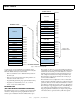
ADSP-TS201S GLOBAL SPACE 0xFFFFFFFF HOST (MSH) 0x80000000 RESERVED 0x74000000 MSSD BANK 3 (MSSD3) 0x70000000 RESERVED EXTERNAL MEMORY SPACE INTERNAL SPACE 0x03FFFFFF RESERVED 0x64000000 MSSD BANK 2 (MSSD2) 0x60000000 RESERVED 0x54000000 MSSD BANK 1 (MSSD1) 0x50000000 RESERVED 0x44000000 MSSD BANK 0 (MSSD0) 0x40000000 BANK 1 (MS1) 0x001F03FF SOC REGISTERS (UREGS) 0x38000000 0x001F0000 BANK 0 (MS0) RESERVED 0x001E03FF 0x30000000 MULTIPROCESSOR MEMORY SPACE INTERNAL REG ISTERS (UREG S) 0x001E0000
ADSP-TS201S The ADSP-TS201S processor provides programmable memory, pipeline depth, and idle cycle for synchronous accesses; and external acknowledge controls to support interfacing to pipelined or slow devices, host processors, and other memorymapped peripherals with variable access, hold, and disable time requirements. Host Interface The ADSP-TS201S processor provides an easy and configurable interface between its external bus and host processors through the external port (see Figure 4).
CONTROL ADDRESS DATA ADDRESS DATA ADSP-TS201S #7 ADSP-TS201S #6 ADSP-TS201S #5 ADSP-TS201S #4 ADSP-TS201S #3 ADSP-TS201S #2 CONTROL ADSP-TS201S ADSP-TS201S #1 001 ID2–0 RST_IN CLKS/REFS LINK DEVICES LINK BR7–2,0 BR1 ADDR31–0 DATA31–0 CONTROL ADSP-TS201S #0 ID2–0 000 RESET RST_IN ADDR31–0 ADDR CLKS/REFS RST_OUT DATA31–0 DATA POR_IN CLOCK SCLK REFERENCE SCLK_VREF REFERENCE VREF SCLKRAT2–0 IRQ3–0 FLAG3–0 LINK LxDATO3–0P/N LxCLKOUTP/N LINK DEVICES (2 MAX) (OPTIONAL) BR7–1 BR0 OE WE
ADSP-TS201S LINK PORTS (LVDS) The DSP’s four full-duplex link ports each provide additional four-bit receive and four-bit transmit I/O capability, using low voltage, differential-signal (LVDS) technology. With the ability to operate at a double data rate—latching data on both the rising and falling edges of the clock—running at up to 500 MHz, each link port can support up to 500M bytes per second per direction, for a combined maximum throughput of 4G bytes per second.
ADSP-TS201S POWER DOMAINS The ADSP-TS201S processor has separate power supply connections for internal logic (VDD), analog circuits (VDD_A), I/O buffer (VDD_IO), and internal DRAM (VDD_DRAM) power supply. Note that the analog (VDD_A) supply powers the clock generator PLLs. To produce a stable clock, systems must provide a clean power supply to power input VDD_A. Designs must pay critical attention to bypassing the VDD_A supply.
ADSP-TS201S eliminating the need to start from the very beginning when developing new application code. The VDK features include threads, critical and unscheduled regions, semaphores, events, and device flags. The VDK also supports priority-based, preemptive, cooperative, and time-sliced scheduling approaches. In addition, the VDK was designed to be scalable. If the application does not use a specific feature, the support code for that feature is excluded from the target system.
ADSP-TS201S PIN FUNCTION DESCRIPTIONS While most of the ADSP-TS201S processor’s input pins are normally synchronous—tied to a specific clock—a few are asynchronous. For these asynchronous signals, an on-chip synchronization circuit prevents metastability problems. Use the ac specification for asynchronous signals when the system design requires predictable, cycle-by-cycle behavior for these signals. The output pins can be three-stated during normal operation.
ADSP-TS201S Table 5. Pin Definitions—External Port Bus Controls Signal ADDR31–0 Description Address Bus. The DSP issues addresses for accessing memory and peripherals on these pins. In a multiprocessor system, the bus master drives addresses for accessing internal memory or I/O processor registers of other ADSP-TS201S processors. The DSP inputs addresses when a host or another DSP accesses its internal memory or I/O processor registers. DATA63–0 I/O/T nc External Data Bus.
ADSP-TS201S Table 6. Pin Definitions—External Port Arbitration Signal BR7–0 Description Multiprocessing Bus Request Pins. Used by the DSPs in a multiprocessor system to arbitrate for bus mastership. Each DSP drives its own BRx line (corresponding to the value of its ID2–0 inputs) and monitors all others. In systems with fewer than eight DSPs, set the unused BRx pins high (VDD_IO). ID2–0 I (pd) na Multiprocessor ID. Indicates the DSP’s ID, from which the DSP determines its order in a multiprocessor system.
ADSP-TS201S Table 7. Pin Definitions—External Port DMA/Flyby Signal DMAR3–0 Type I/A Term epu Description DMA Request Pins. Enable external I/O devices to request DMA services from the DSP. In response to DMARx, the DSP performs DMA transfers according to the DMA channel’s initialization. The DSP ignores DMA requests from uninitialized channels. IOWR O/T nc I/O Write. When a DSP DMA channel initiates a flyby mode read transaction, the DSP (pu_0) asserts the IOWR signal during the data cycles.
ADSP-TS201S Table 8. Pin Definitions—External Port SDRAM Controller Signal MSSD3–0 Type I/O/T (pu_0) Term nc Description Memory Select SDRAM. MSSD0, MSSD1, MSSD2, or MSSD3 is asserted whenever the DSP accesses SDRAM memory space. MSSD3–0 are decoded memory address pins that are asserted whenever the DSP issues an SDRAM command cycle (access to ADDR31:30 = 0b01—except reserved spaces shown in Figure 3 on Page 6). In a multiprocessor system, the master DSP drives MSSD3–0. RAS I/O/T nc Row Address Select.
ADSP-TS201S Table 9. Pin Definitions—JTAG Port Signal EMU TCK TDI TDO TMS TRST Description Emulation. Connected to the DSP’s JTAG emulator target board connector only. Test Clock (JTAG). Provides an asynchronous clock for JTAG scan. Test Data Input (JTAG). A serial data input of the scan path. Test Data Output (JTAG). A serial data output of the scan path. Test Mode Select (JTAG). Used to control the test state machine. Test Reset (JTAG). Resets the test state machine.
ADSP-TS201S Table 11. Pin Definitions—Link Ports Signal LxDATO3–0P LxDATO3–0N LxCLKOUTP LxCLKOUTN LxACKI Type O O O O I (pd) Term nc nc nc nc nc Description Link Ports 3–0 Data 3–0 Transmit LVDS P Link Ports 3–0 Data 3–0 Transmit LVDS N Link Ports 3–0 Transmit Clock LVDS P Link Ports 3–0 Transmit Clock LVDS N Link Ports 3–0 Receive Acknowledge. Using this signal, the receiver indicates to the transmitter that it may continue the transmission. LxBCMPO O (pu) nc Link Ports 3–0 Block Completion.
ADSP-TS201S Table 13. Impedance Control Selection CONTROLIMP1-0 00 (recommended) 01 10 (default) 11 Driver Mode Normal Reserved A/D Mode Reserved Table 14. Drive Strength/Output Impedance Selection DS2–0 Pins 000 001 010 011 100 101 (default) 110 111 1 2 Drive Strength1 Strength 0 (11.1%) Strength 1 (23.8%) Strength 2 (36.5%) Strength 3 (49.2%) Strength 4 (61.9%) Strength 5 (74.6%) Strength 6 (87.
ADSP-TS201S STRAP PIN FUNCTION DESCRIPTIONS Some pins have alternate functions at reset. Strap options set DSP operating modes. During reset, the DSP samples the strap option pins. Strap pins have an internal pull-up or pull-down for the default value. If a strap pin is not connected to an overdriving external pull-up, pull-down, or logic load, the DSP samples the default value during reset.
ADSP-TS201S ADSP-TS201S—SPECIFICATIONS Note that component specifications are subject to change without notice. For information on link port electrical characteristics, see Link Port Low Voltage, Differential-Signal (LVDS) Electrical Characteristics, and Timing on Page 30. OPERATING CONDITIONS Parameter Description Test Conditions Grade1 Min Typ Max Unit VDD Internal Supply Voltage @ CCLK = 600 MHz 060 1.14 1.20 1.26 V @ CCLK = 500 MHz 050 1.00 1.05 1.10 V @ CCLK = 600 MHz 060 1.
ADSP-TS201S Table 18. Maximum Duty Cycle for Input Transient Voltage VIN Max (V)1 +3.63 +3.64 +3.70 +3.78 +3.86 +3.93 Maximum Duty Cycle2 100% 90% 50% 30% 17% 10% VIN Min (V)1 –0.33 –0.34 –0.40 –0.48 –0.56 –0.63 1 The individual values cannot be combined for analysis of a single instance of overshoot or undershoot.
ADSP-TS201S PACKAGE INFORMATION ABSOLUTE MAXIMUM RATINGS The information presented in Figure 8 provide details about the package branding for the ADSP-TS201S processors. For a complete listing of product availability, see Ordering Guide on Page 46. Stresses greater than those listed below may cause permanent damage to the device. These are stress ratings only.
ADSP-TS201S TIMING SPECIFICATIONS With the exception of DMAR3–0, IRQ3–0, TMR0E, and FLAG3–0 (input only) pins, all ac timing for the ADSP-TS201S processor is relative to a reference clock edge. Because input setup/hold, output valid/hold, and output enable/disable times are relative to a clock edge, the timing data for the ADSPTS201S processor has few calculated (formula-based) values. For information on ac timing, see General AC Timing.
ADSP-TS201S Table 23. Reference Clocks—System Clock (SCLK) Cycle Time Parameter tSCLK1, 2, 3 tSCLKH tSCLKL tSCLKF tSCLKR tSCLKJ5, 6 Description System Clock Cycle Time System Clock Cycle High Time System Clock Cycle Low Time System Clock Transition Time—Falling Edge4 System Clock Transition Time—Rising Edge System Clock Jitter Tolerance SCLKRAT = 4×, 6×, 8×, 10×, 12× Min Max 8 50 0.40 × tSCLK 0.60 × tSCLK 0.40 × tSCLK 0.60 × tSCLK — 1.5 — 1.5 — 500 SCLKRAT = 5×, 7× Min Max 8 50 0.45 × tSCLK 0.
ADSP-TS201S Table 25. Power-Up Timing1 Parameter Timing Requirement tVDD_DRAM VDD_DRAM Stable After VDD, VDD_A, VDD_IO Stable 1 Min Max >0 Unit ms For information about power supply sequencing and monitoring solutions, please visit www.analog.com/sequencing. tVDD_DRAM VDD VDD_A VDD_IO VDD_DRAM Figure 12. Power-Up Timing Table 26.
ADSP-TS201S Table 27. Normal Reset Timing Parameter Min Max Unit Timing Requirements tRST_IN RST_IN Asserted 2 ms tSTRAP RST_IN Deasserted After Strap Pins Stable 1.5 ms 1.5 ms Switching Characteristic tRST_OUT RST_OUT Deasserted After RST_IN Deasserted tRST_IN RST_IN tRST_OUT RST_OUT tSTRAP STRAP PINS Figure 14. Normal Reset Timing Table 28. On-Chip DRAM Refresh1 Parameter Min Max Unit 1.
ADSP-TS201S Table 29. AC Signal Specifications Rev.
ADSP-TS201S Table 29. AC Signal Specifications (Continued) Output Valid (Max) Output Hold (Min) Output Enable (Min)1 Output Disable (Max)1 Reference Clock Description Static Pins—Must Be Constant Static Pins—Must Be Constant Static Pins—Must Be Connected to VSS Strap Pins JTAG System Pins Input Hold (Min) Name DS2–08 SCLKRAT2–08 ENEDREG STRAP SYS9, 10 JTAG SYS11, 12 Input Setup (Min) (All values in this table are in nanoseconds.) — — — 1.5 +2.5 — — — 0.5 +10.0 — — — — +12.0 — — — — –1.
ADSP-TS201S Link Port Low Voltage, Differential-Signal (LVDS) Electrical Characteristics, and Timing Table 30 and Table 31 with Figure 16 provide the electrical characteristics for the LVDS link ports. The LVDS link port signal definitions represent all differential signals with a VOD = 0 V level and use signal naming without N (negative) and P (positive) suffixes (see Figure 17). Table 30.
ADSP-TS201S Link Port—Data Out Timing Table 32 with Figure 18, Figure 19, Figure 20, Figure 21, Figure 22, and Figure 23 provide the data out timing for the LVDS link ports. Table 32.
ADSP-TS201S tLCLKOP VOD = 0V LxCLKOUT LxCLKOUT tLCLKOH tCOJT VOD = 0V tLCLKOL tLDOS tLDOH tLDOS tLDOH Figure 18. Link Ports—Output Clock LxDATO VOD = 0V VO_P RL RL = 100⍀ CL_P CL Figure 20. Link Ports—Data Output Setup and Hold1 CL = 0.1pF CL_P = 5pF 1 CL_N = 5pF VO_N These parameters are valid for both clock edges. CL_N tREO tFEO | | + VOD MIN VOD = 0V -|VOD| MIN Figure 19.
ADSP-TS201S FIRST EDGE OF 5TH SHORT WORD IN A QUAD WORD LAST EDGE IN A QUAD WORD LxCLKOUT VOD = 0V LxDATO VOD = 0V tLACKIS tLACKIH LxACKI tBCMPOH LxBCMPO Figure 22. Link Ports—Transmission End and Stops LAST EDGE IN A QUAD WORD LxCLKOUT VOD = 0V LxDATO VOD = 0V tLACKIS tLACKIH LxACKI Figure 23. Link Ports—Back to Back Transmission Rev.
ADSP-TS201S Link Port—Data In Timing Table 33 with Figure 24 and Figure 25 provide the data in timing for the LVDS link ports. Table 33. Link Port—Data In Timing Parameter Inputs tLCLKIP Description Min LxCLKIN Period (Figure 25) Greater of 1.8 or 0.9 × tCCLK1 0.201, 2 0.251, 3 0.301, 4 0.351, 5 0.201, 2 0.251, 3 0.301, 4 0.
ADSP-TS201S tLCLKIP LxCLKIN VOD = 0V tLDIS tLDIH tLDIS tLDIH LxDATI VOD = 0V Figure 25. Link Ports—Data Input Setup and Hold 1 1 These parameters are valid for both clock edges. Rev.
ADSP-TS201S OUTPUT DRIVE CURRENTS STRENGTH 0 15.0 12.5 STRENGTH 2 45 IOL 36 27 OUTPUT PIN CURRENT (mA) Figure 26 through Figure 33 show typical I–V characteristics for the output drivers of the ADSP-TS201S processor. The curves in these diagrams represent the current drive capability of the output drivers as a function of output voltage over the range of drive strengths. Typical drive currents for intermediate temperatures (such as 85°C) should be obtained from the curves using linear interpolation.
ADSP-TS201S TEST CONDITIONS STRENGTH 5 OUTPUT PIN CURRENT (mA) 88 77 66 The ac signal specifications (timing parameters) appear in Table 29 on Page 28. These include output disable time, output enable time, and capacitive loading. The timing specifications for the DSP apply for the voltage reference levels in Figure 34. IOL 55 44 33 VDD_IO = 2.63V, –40°C VDD_IO = 2.5V, +25°C 22 11 0 VDD_IO = 2.63V, –40°C VDD_IO = 2.38V, +105°C –11 –22 INPUT OR OUTPUT VDD_IO = 2.5V, +25°C 1.25V VDD_IO = 2.
ADSP-TS201S Output Enable Time STRENGTH 1 The output enable time tENA is the difference between tMEASURED_ENA and tRAMP as shown in Figure 35. The time tMEASURED_ENA is the interval from when the reference signal switches to when the output voltage ramps ΔV from the measured three-stated output level. tRAMP is calculated with test load CL, drive current ID, and with ΔV equal to 0.4 V. Capacitive Loading Output valid and hold are based on standard capacitive loads: 30 pF on all pins (see Figure 36).
ADSP-TS201S STRENGTH 4 STRENGTH 7 (VDD_IO = 2.5V) (VDD_IO = 2.5V) 25 RISE AND FALL TIMES (ns) RISE AND FALL TIMES (ns) 25 20 15 10 FALL TIME Y = 0.0592x + 1.0629 20 15 10 RISE TIME 5 5 Y = 0.0321x + 0.6512 FALL TIME Y = 0.0313x + 0.818 RISE TIME Y = 0.0573x + 0.9789 0 0 10 20 30 40 50 60 70 80 LOAD CAPACITANCE (pF) 90 0 100 0 10 20 30 40 50 60 70 80 LOAD CAPACITANCE (pF) 90 100 Figure 44. Typical Output Rise and Fall Time (10% to 90%, VDD_IO = 2.5 V) vs.
ADSP-TS201S ENVIRONMENTAL CONDITIONS The ADSP-TS201S processor is rated for performance under TCASE environmental conditions specified in the Operating Conditions on Page 21. Thermal Characteristics The ADSP-TS201S processor is packaged in a 25 mm × 25 mm, thermally enhanced ball grid array (BGA_ED). The ADSP-TS201S processor is specified for a case temperature (TCASE). To ensure that the TCASE data sheet specification is not exceeded, a heat sink and/or an air flow source may be required.
ADSP-TS201S 576-BALL BGA_ED PIN CONFIGURATIONS Figure 46 shows a summary of pin configurations for the 576-ball BGA_ED package and Table 35 lists the signal-to-ball assignments. 2 1 4 3 6 5 8 7 10 9 14 12 11 13 16 15 20 18 17 19 22 21 24 23 A B C D E F G H KEY: J K SIGNAL L VDD M VDD_IO N P VDD_DRAM R VDD_A T VREF U VSS V NO CONNECT W Y AA AB AC AD TOP VIEW Figure 46.
ADSP-TS201S Table 35. 576-Ball (25 mm × 25 mm) BGA_ED Ball Assignments Ball No.
ADSP-TS201S Table 35. 576-Ball (25 mm × 25 mm) BGA_ED Ball Assignments (Continued) Ball No.
ADSP-TS201S Table 35. 576-Ball (25 mm × 25 mm) BGA_ED Ball Assignments (Continued) Ball No.
ADSP-TS201S OUTLINE DIMENSIONS The ADSP-TS201S processor is available in a 25 mm × 25 mm, 576-ball metric thermally enhanced ball grid array (BGA_ED) package with 24 rows of balls (BP-576). 25.20 25.00 24.80 24 22 20 18 16 14 12 10 8 6 4 2 23 21 19 17 15 13 11 9 7 5 3 1 B 1.25 1.00 0.75 1.00 BSC A1 BALL INDICATOR D F H 25.20 25.00 24.80 23.00 BSC SQ K M P 1.00 BSC (BALL PITCH) T V Y AB AD 1.25 1.00 0.75 1.00 BSC TOP VIEW 3.10 2.94 2.78 C E G J L N R U W AA AC BOTTOM VIEW DETAIL A 1.
ADSP-TS201S ORDERING GUIDE Model ADSP-TS201SABP-060 ADSP-TS201SABP-050 ADSP-TS201SYBP-050 ADSP-TS201SABPZ0603 ADSP-TS201SABPZ0503 ADSP-TS201SYBPZ0503 Temperature Range1 –40°C to +85°C –40°C to +85°C –40°C to +105°C –40°C to +85°C –40°C to +85°C –40°C to +105°C Instruction Rate2 600 MHz 500 MHz 500 MHz 600 MHz 500 MHz 500 MHz On-Chip DRAM 24M bit 24M bit 24M bit 24M bit 24M bit 24M bit Operating Voltage 1.20 VDD, 2.5 VDD_IO, 1.6 VDD_DRAM 1.05 VDD, 2.5 VDD_IO, 1.5 VDD_DRAM 1.05 VDD, 2.5 VDD_IO, 1.
ADSP-TS201S Rev.
ADSP-TS201S ©2006 Analog Devices, Inc. All rights reserved. Trademarks and registered trademarks are the property of their respective owners. D04324-0-11/06(C) Rev.