
- Analog Devices, Inc. Embedded Processor Specification Sheet


Rev. C | Page 26 of 48 | December 2006
ADSP-TS201S
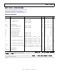
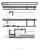
Table 25. Power-Up Timing
1
Parameter Min Max Unit
Timing Requirement
t
VDD_DRAM
V
DD_DRAM
Stable After V
DD
, V
DD_A
, V
DD_IO
Stable >0 ms
1
For information about power supply sequencing and monitoring solutions, please visit www.analog.com/sequencing.
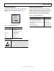
Figure 12. Power-Up Timing
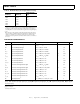
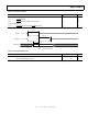
Table 26. Power-Up Reset Timing
Parameter Min Max Unit
Timing Requirements
t
RST_IN_PWR
RST_IN Deasserted After V
DD
, V
DD_A
, V
DD_IO
, V
DD_DRAM
, SCLK, and Static/
Strap Pins Stable 2 ms
t
TRST_IN_PWR
1
TRST Asserted During Power-Up Reset 100 × t
SCLK
ns
Switching Characteristic
t
RST_OUT_PWR
RST_OUT Deasserted After RST_IN Deasserted 1.5 ms
1
Applies after V
DD
, V
DD_A
, V
DD_IO
, V
DD_DRAM
, and SCLK are stable and before RST_IN deasserted.
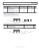
Figure 13. Power-Up Reset Timing
V
DD
V
DD_A
V
DD_IO
V
DD_DRAM
t
VDD_DRAM
RST_OUT
t
RST_OUT_PWR
TRST
t
TRST_IN_PWR
SCLK, V
DD,
V
DD_A ,
V
DD_IO,
V
DD_DRAM
STATIC/STRAP PINS
RST_IN
t
RST_IN_PWR