
Datasheet


TMP03/TMP04
REV. A
–10–
APPLICATIONS INFORMATION
Supply Bypassing
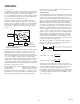
Precision analog products, such as the TMP03, require a well-
filtered power source. Since the TMP03 operate from a single 5
V supply, it seems convenient to simply tap into the digital logic
power supply. Unfortunately, the logic supply is often a switch-
mode design, which generates noise in the 20 kHz to 1 MHz
range. In addition, fast logic gates can generate glitches hundred
of millivolts in amplitude due to wiring resistance and induc-
tance.
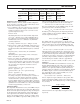
If possible, the TMP03 should be powered directly from the
system power supply. This arrangement, shown in Figure 3, will
isolate the analog section from the logic switching transients. Even
if a separate power supply trace is not available, however, gener-
ous supply bypassing will reduce supply-line induced errors.
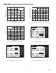
Local supply bypassing consisting of a 10 µF tantalum electro-
lytic in parallel with a 0.1 µF ceramic capacitor is recommended
(Figure 4a).
TTL/CMOS
LOGIC
CIRCUITS
TMP03/
TMP04
10F
TANT
0.1F
5V
POWER SUPPLY
+
Figure 3. Use Separate Traces to Reduce Power Supply
Noise
TMP03/
TMP04
10F 0.1F
V+
D
OUT
GND
5V
TMP03/
TMP04
10F 0.1F
V+
D
OUT
GND
5V
50
a. b.
Figure 4. Recommended Supply Bypassing for the
TMP03
The quiescent power supply current requirement of the TMP03
is typically only 900 µA. The supply current will not change
appreciably when driving a light load (such as a CMOS gate), so
a simple RC filter can be added to further reduce power supply
noise (Figure 4b).
TMP03 Output Configurations
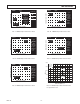
The TMP03 (Figure 5a) has an open-collector NPN output
which is suitable for driving a high current load, such as an
opto-isolator. Since the output source current is set by the pull-
up resistor, output capacitance should be minimized in TMP03
applications. Otherwise, unequal rise and fall times will skew the
pulsewidth and introduce measurement errors. The NPN tran-
sistor has a breakdown voltage of 18 V.
V+
D
OUT
D
OUT
TMP03
TMP04
a. b.
Figure 5. TMP03 Digital Output Structure
The TMP04 has a “totem-pole” CMOS output (Figure 5b) and
provides rail-to-rail output drive for logic interfaces. The rise
and fall times of the TMP04 output are closely matched, so that
errors caused by capacitive loading are minimized. If load ca-
pacitance is large, for example when driving a long cable, an
external buffer may improve accuracy. See the “Remote Tem-
perature Measurement” section of this data sheet for
suggestions.
Interfacing the TMP03 to Low Voltage Logic
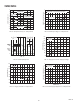
The TMP03’s open-collector output is ideal for driving logic
gates that operate from low supply voltages, such as 3.3 V. As
shown in Figure 6, a pull-up resistor is connected from the low
voltage logic supply (2.9 V, 3 V, etc.) to the TMP03 output.
Current through the pull-up resistor should be limited to about
1 mA, which will maintain an output LOW logic level of
<200 mV.
TMP03
5V
D
OUT
GND
3.3V
3.3k
V+
TO LOW VOLTAGE
LOGIC GATE INPUT
Figure 6. Interfacing to Low Voltage Logic
Remote Temperature Measurement
When measuring a temperature in situations where high com-
mon-mode voltages exist, an opto-isolator can be used to isolate
the output (Figure 7a). The TMP03 is recommended in this
application because its open-collector NPN transistor has a
higher current sink capability than the CMOS output of the
TMP04. To maintain the integrity of the measurement, the
opto-isolator must have relatively equal turn-on and turn-off
times. Some Darlington opto-isolators, such as the 4N32, have
a turn-off time that is much longer than their turn-on time. In
this case, the T1 time will be longer than T2, and an erroneous
reading will result. A PNP transistor can be used to provide
greater current drive to the opto-isolator (Figure 7b). An opto-
isolator with an integral logic gate output, such as the H11L1
from Quality Technology, can also be used (Figure 8).