
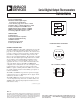
Datasheet
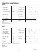
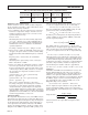


Parameter Symbol Conditions Min Typ Max Unit
ACCURACY
Temperature Error –25°C < T
A
< +100°C
1
1.5 4.0 °C
–40°C < T
A
< –25°C
1
2.0 5.0 °C
Temperature Linearity 0.5 °C
Long-Term Stability 1000 Hours at 125°C 0.5 °C
Nominal Mark-Space Ratio T1/T2 T
A
= 0°C 58.8 %
Nominal T1 Pulsewidth T1 10 ms
Power Supply Rejection Ratio PSRR Over Rated Supply 0.7 1.4 °C/V
T
A
= 25°C
OUTPUTS
Output Low Voltage V
OL
I
SINK
= 1.6 mA 0.2 V
Output Low Voltage V
OL
I
SINK
= 5 mA 2 V
0°C < T
A
< 100°C
Output Low Voltage V
OL
I
SINK
= 4 mA 2 V
–40°C < T
A
< 0°C
Digital Output Capacitance C
OUT
(Note 2) 15 pF
Fall Time t
HL
See Test Load 150 ns
Device Turn-On Time 20 ms
POWER SUPPLY
Supply Range V+ 4.5 7 V
Supply Current I
SY
Unloaded 0.9 1.3 mA
NOTES
1
Maximum deviation from output transfer function over specified temperature range.
2
Guaranteed but not tested.
Specifications subject to change without notice.
Test Load
10 kΩ to 5 V Supply, 100 pF to Ground
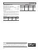
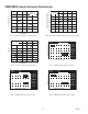
TMP04F
Parameter Symbol Conditions Min Typ Max Unit
ACCURACY
Temperature Error T
A
= 25°C 1.0 3.0 °C
–25°C < T
A
< +100°C
1
1.5 4.0 °C
–40°C < T
A
< –25°C
1
2.0 5.0 °C
Temperature Linearity 0.5 °C
Long-Term Stability 1000 Hours at 125°C 0.5 °C
Nominal Mark-Space Ratio T1/T2 T
A
= 0°C 58.8 %
Nominal T1 Pulsewidth T1 10 ms
Power Supply Rejection Ratio PSRR Over Rated Supply 0.7 1.2 °C/V
T
A
= 25°C
OUTPUTS
Output High Voltage V
OH
I
OH
= 800 µA V+ –0.4 V
Output Low Voltage V
OL
I
OL
= 800 µA 0.4 V
Digital Output Capacitance C
OUT
(Note 2) 15 pF
Fall Time t
HL
See Test Load 200 ns
Rise Time t
LH
See Test Load 160 ns
Device Turn-On Time 20 ms
POWER SUPPLY
Supply Range V+ 4.5 7 V
Supply Current I
SY
Unloaded 0.9 1.3 mA
NOTES
1
Maximum deviation from output transfer function over specified temperature range.
2
Guaranteed but not tested.
Specifications subject to change without notice.
Test Load
100 pF to Ground
REV. A
TMP03/TMP04–SPECIFICATIONS
TMP03F
(V+ = 5 V, –40C ≤ T
A
≤ 100C, unless otherwise noted.)
–2–
(V+ = 5 V, –40C ≤ T
A
≤ 100C, unless otherwise noted.)