F1DQ3007 Bluetooth v5.0 Dual module F1DQ3007 Datasheet Confidential / Preliminary Documentation Revision 1.
F1DQ3007 Bluetooth v5.0 Dual module List of Contents 1. General 1.1 Overview 1.2 Features 1.3 Application 1.4 Pinout Diagram 1.5 Device Terminal Functions 1.6 Module Dimension 2. Characteristics 2.1 Electrical Characteristics 2.2 RF Characteristics 2.3 Audio Characteristics 2.4 ESD Protection 3. Interface 3.1 UART interface 3.2 USB interface 3.3 Programming and debug interface 3.4 3.5 3.6 3.7 3.8 I2C interface LED drivers Audio interfaces Battery Charger Reset, RST# 4. Application Schematic 5.
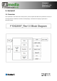
F1DQ3007 Bluetooth v5.0 Dual module 1. General 1.1 Overview This specification covers Bluetooth module (class-1) which complies with Bluetooth specification version 5.0 and integrates RF & Baseband controller in small package. This Module has deployed Qualcomm’s QCC3007 chipset.
F1DQ3007 Bluetooth v5.0 Dual module 1.2 Features • Bluetooth supports . Bluetooth 5.0 specification compliant . RF performance of 9dbm Transmitter power . -92dBm Basic rate Receiver sensitivity.(QCC3007 Chipset only) . Internal Chip Antenna • Kalimba DSP . Qualcomm Kalimba DSP (80MIPS) • Audio Interface . Dual I2S and PCM . SPDIF . Analog and Digital microphone • Physical interfaces . UART/USB(2.0) . 14 general PIO . 2 x PCM/I2S . 1 SPDIF interfaces . 3 LED drivers • Memory . On-chip Rom, .
F1DQ3007 Bluetooth v5.0 Dual module 1.
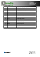
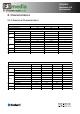
F1DQ3007 Bluetooth v5.0 Dual module 1.5 Device Terminal Functions Pad Pin Name Pin Description 1 GND GROUND 2 GND GROUND 3 AIO[0] Analog programmable input line 0.
F1DQ3007 Bluetooth v5.0 Dual module 31 PIO[8] Alternative function: ■UART_RTS ■I2S2_SD_IN 32 PIO[6] Alternative function: ■I2S2_SD_OUT 33 VDD_PADS2 Positive supply input for input/output ports.
F1DQ3007 Bluetooth v5.0 Dual module 1.5.1 Programmable I/O ports(PIO) F1DQ3007 provides up to 14 lines of programmable bidirectional I/O, PIO[21,18:16,9:0] Table 1.
F1DQ3007 Bluetooth v5.0 Dual module 1.
F1DQ3007 Bluetooth v5.0 Dual module 2. Characteristics 2.1.1 Electrical Characteristics Absolute maximum ratings Rating Storage temperature Supply voltage 5V 3.3V Battery PIO 1.8V 1.35V VBUS SMP_BYP VDD_USB LED[2:0] SMP_BAT VBAT_SENSE VREGENABLE VDD_PADS1 VDD_PADS2 SMPS_1V8 SMPS_1V35 Other Teminal Voltage Min -40 Max 105 Unit ℃ -0.4 -0.4 -0.4 -0.4 -0.4 -0.4 -0.4 -0.4 -0.4 -0.4 -0.4 6.50 3.60 3.60 4.40 4.40 4.40 4.40 3.60 3.60 1.95 1.45 V V V V V V V V V V V VSS -0.4 VDD +0.
F1DQ3007 Bluetooth v5.0 Dual module 2.1.2 Power consumption DUT role N/A N/A N/A Master Master Master Master Master Master Master Master Master Master Slave Slave Slave Slave Slave Slave Slave Slave Slave Slave Master Slave N/A N/A N/A N/A Connection Deep sleep With UART host connection Page = 1280 ms interval Page scan Window = 11.25 ms Inquiry = 1280 ms interval Inquiry and Page = 1280 ms interval page scan Window = 11.
F1DQ3007 Bluetooth v5.0 Dual module 2.2 RF Characteristics 2.2.
F1DQ3007 Bluetooth v5.0 Dual module 2.2.
F1DQ3007 Bluetooth v5.0 Dual module 2.3 Audio Characteristics 2.3.1 Stereo codec: analog-to-digital converter Analog-to-digital converter Conditions Parameter Resolution Input sample rate, Fsample Maximum ADC input signal 0 dB = 1600 mVpk-pk amplitude Min - Typ - Max 16 Unit Bits 8 - 48 kHz 13 - - 94.4 92.4 92.5 93.2 91.9 2260 mVpk-pk Fsample SNR fin = 1 kHz B/W = 20 Hz→Fsample/2 (20 kHz max) A - Weighted THD+N < 0.1% 1.6 Vpk-pk input 8 kHz 16 kHz 32 kHz 44.
F1DQ3007 Bluetooth v5.0 Dual module 2.3.1 Stereo codec: digital-to-analog converter Digital-to-analog converter Condition Parameter Resolution Output sample rate, Fsample SNR THD+N fin = 1 kHz B/W = 20 Hz → 20 kHz A - Weighted THD+N < 0.
F1DQ3007 Bluetooth v5.0 Dual module 3. Interface 3.1 UART interface Four signals are used to implement the UART function. This is only for test and debug. UART_TX and UART_RX transfer data between the two devices. The remaining two signals, UART_CTS and UART_RTS, can be used to implement RS232 hardware flow control where both are active low indicators. 3.1.1 UART Setting User can change data format the following selection using PSKEY.
F1DQ3007 Bluetooth v5.0 Dual module . Wake on Bluetooth, includes permitted devices and set-up prior to selective suspend . Suspend mode current draw . PIO status in suspend mode . Resume, detach and wake PIOs - Battery charging from USB, which describes dead battery provision, charge currents, charging in suspend modes and USB VBUS voltage consideration 3.3 Programming and Debug interface F1DQ3007 provides a debug SPI interface for programming, configuring, and debugging the F1DQ3007.
F1DQ3007 Bluetooth v5.0 Dual module 3.6 Audio Interfaces F1DQ3007’s audio interface consists below. ■ Dual analog audio inputs ■ Dual analog audio outputs ■ 1 digital microphone input ■ 2 configurable I²S interfaces ■ Configurable SPDIF input interface 3.6.1 Analog Input F1DQ3007 contains an independent low-noise microphone bias generator. In using Line input, F1DQ3007 supports a differential input and a single-ended input.
F1DQ3007 Bluetooth v5.0 Dual module 3.6.2 Audio Output The output stage digital circuitry converts the signal from 16 bit per sample, linear PCM of variable sampling frequency to bit stream, which is fed into the analog output circuitry. The analog output circuit comprises a DAC, a buffer with gain-setting, a low pass filter, and a class AB output stage amplifier. SPKR_RN SPKR_RP SPKR_LN SPKR_LP Mono operation is a single-channel operation of the stereo codec.
F1DQ3007 Bluetooth v5.0 Dual module 3.7 Battery Charger 3.7.1 Battery Charger Hardware Operating Modes The battery charger has 5 modes. - Disabled - Trickle charge - Fast charge - Standby : fully charged or float charge - Error : charging input voltage. The battery charger operating mode is determined by the battery voltage and current. The internal charger circuit can provide up to 200mA. For currents higher than this, external pass transistor is need. 3.7.1.
F1DQ3007 Bluetooth v5.0 Dual module 3.8 Reset, RST# QCC3007 QFN is reset from several sources: ■ RST# pin ■ Power-on reset ■ USB charger attach reset ■ Software configured watchdog timer The RST# pin is an active low reset. Assert the reset signal for a period > 5 ms to ensure a full reset. At reset the digital I/O pins are set to inputs for bidirectional pins and outputs are set to tristate.
F1DQ3007 Bluetooth v5.0 Dual module 4.
F1DQ3007 Bluetooth v5.
F1DQ3007 Bluetooth v5.0 Dual module 5. Antenna spec 5.
F1DQ3007 Bluetooth v5.0 Dual module 5.2 Active measurement data(T.B.
F1DQ3007 Bluetooth v5.0 Dual module 6. Module Placement Rule On the main PCB, the areas under the antenna should not contain any top, inner layer, or bottom copper as shown in Figure. For the best range performance, keep all external metal away from the chip antenna at least 45 mm. In all cases, the performance of the antenna can vary depending on GND.
F1DQ3007 Bluetooth v5.0 Dual module 7.
F1DQ3007 Bluetooth v5.0 Dual module 8. Reflow Temperature Profile - Please use the reflow within 2 times.
F1DQ3007 Bluetooth v5.0 Dual module 9. Packing information a.
F1DQ3007 Bluetooth v5.
F1DQ3007 Bluetooth v5.0 Dual module b. Barcode(T.B.
10. FCC Statement FCC Part 15C 15.247, 15E 15.407 is applied to the modular transmitter. Federal Communication Commission Interference Statement This equipment has been tested and found to comply with the limits for a Class B digital device, pursuant to Part 15 of the FCC Rules. These limits are designed to provide reasonable protection against harmful interference in a residential installation.
IMPORTANT NOTE: FCC Radiation Exposure Statement: This equipment complies with FCC radiation exposure limits set forth for an uncontrolled environment. This equipment should be installed and operated with minimum distance 20cm between the radiator & your body. This module is intended for OEM integrator. The OEM integrator is still responsible for the FCC compliance requirement of the end product, which integrates this module.
11. IC Statement This Class B digital apparatus complies with Canadian ICES-003. This device complies with Industry Canada license-exempt RSS standard(s). Operation is subject to the following two conditions: (1) this device may not cause interference, and (2) this device must accept any interference, including interference that may cause undesired operation of the device. Cet appareil numérique de la classe B est conforme á la norme NMB-003 du Canada.
This module is intended for OEM integrator. The OEM integrator is still responsible for the IC compliance requirement of the end product, which integrates this module. USERS MANUAL OF THE END PRODUCT: In the users manual of the end product, the end user has to be informed to keep at least 20cm separation with the antenna while this end product is installed and operated. The end user has to be informed that the IC radio-frequency exposure guidelines for an uncontrolled environment can be satisfied.
F1DQ3007 Bluetooth v5.0 Dual module 12. Revision History Revision Date Change Descriptions Rev 1.0 2019-07-10 Initial release T.G.KIM Rev1.1 2019-08-21 Change Name / Pinmap / Application SCH T.G.KIM Rev1.2 2019-09-11 Electrical data T.G.KIM Rev1.3 2019-09-16 Operating Temperature Range update & Issued by T.G.KIM Keep out area update Rev1.4 2019-10-01 Add Module Placement Rule Rev1.5 2019-10-29 Add Audio Characteristics T.G.KIM Rev1.6 2019-12-12 Dimension & modify T.G.KIM J.