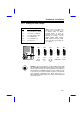
Chapter 2 Hardware Installation This chapter gives you a step-by-step procedure on how to install your system. Follow each section accordingly. Caution: Electrostatic discharge (ESD) can damage your processor, disk drives, expansion boards, and other components. Always observe the following precautions before you install a system component. 1. Do not remove a component from its protective packaging until you are ready to install it. 2.
Hardware Installation 2.
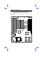
Hardware Installation Jumpers: JP1,JP2: JP3,JP4: JP7: JP8: JP9,JP10, JP11,JP12 JP14: JP18: JP20: JP25: CPU frequency ratio select CPU external (bus) clock select CPU core voltage setting (Vcore) I/O voltage setting (Vio) CPU type (Single/Dual voltage, Vcpuio) selection For clearing CMOS Enable/disable onboard super I/O controller Enable/disable onboard PS/2 mouse DIMM memory type select Connectors: KB1: PWR1: PS2 MS: USB: COM1: COM2: FDC1: PRINTER: IDE1: IDE2: FAN: IrDA: HDD LED: PANEL: AT keyboard conne
Hardware Installation 2.2 Jumper Settings Board jumpers are made of pin headers and plastic connecting caps. These are included in the mainboard design to enable you to customize your hardware. The onboard jumpers are normally set to its default and optimum setting. Be sure you have basic knowledge of computer hardware and understand the function of the jumper before you change any setting. Pin 1 of a jumper is indicated by a bold line on the mainboard.
Hardware Installation 2.2.1 Setting the CPU Voltage JP7 CPU Core Voltage (Vcore) 1-2 3-4 5-6 7-8 9-10 11-12 3.45V (Intel P54C or IDT C6) 3.52V (Cyrix or AMD K5) 2.9V (K6-166/200 or M2) 2.8V (MMX P55C) 3.2V (AMD K6-233) 2.1V (Reserved) JP7 JP7 1 3 5 7 9 11 JP7 is used to select CPU core voltage (Vcore), normally it is set to default 3.45V for INTEL Pentium P54C.
Hardware Installation JP8 1-2 3-4 2-6 JP8 is reserved for testing purposes only. This jumper enables you to set the voltage of the onboard chipset and PBSRAM (Vio). For dual-voltage CPU, JP8 also functions as CPU I/O voltage (Vcpuio) controller. The default voltage setting is 3.45V. I/O Voltage (Vio) 3.45V (default) 3.52V JP8 JP8 1 2 1 2 3 4 3 4 3.45V (default) 3.
Hardware Installation JP9 JP10 JP11 JP12 CPU Type (Vcpuio) 1-2 & 3-4 Open 1-2 & 3-4 Open Single Voltage CPU Vcpuio = Vcore (default) Open 1-2 & 3-4 Open 1-2 & 3-4 Dual Voltage CPU Vcpuio = Vio (PP/MT P55C) Set the jumpers JP9, JP10, JP11, and JP12 according to the type of CPU currently supported. These jumpers are actually for selecting the CPU I/O voltage (Vcpuio). Normally, for single-voltage CPU such as P54C, AMD K5 and Cyrix 6x86, Vcpuio is equal to Vcore.
Hardware Installation CPU Type Vcore Vio Vcpuio JP7 JP8 JP9 JP10 JP11 JP12 Intel P54C 3.45V 3.45V Vcore 1-2 1-2 1-2, 3-4 Open 1-2, 3-4 Open Intel MMX (P55C) 2.8V 3.45V Vio 7-8 1-2 Open 1-2, 3-4 Open 1-2, 3-4 AMD K5 (Single voltage) 3.52V 3.45V Vcore 3-4 1-2 1-2, 3-4 Open 1-2, 3-4 Open AMD K6166/200 2.9V 3.45V Vio 5-6 1-2 Open 1-2, 3-4 Open 1-2, 3-4 AMD K6-233 3.2V 3.45V Vio 9-10 1-2 Open 1-2, 3-4 Open 1-2, 3-4 Cyrix 6x86 3.52V 3.
Hardware Installation 2.2.2 Selecting the CPU Frequency JP1 JP2 1-2 2-3 2-3 1-2 1-2 1-2 2-3 2-3 CPU Frequency Ratio 1.5x (3.5x) 2x 2.5x (1.75x) 3x The Intel Pentium, Cyrix 6x86 and AMD K5/K6 CPUs have different internal (Core) and external (Bus) frequency. The ratio of Core/Bus frequency that the CPU uses to multiply the external clock and produce internal frequency is selected by setting JP1 and JP2. Core frequency = Ratio x External bus clock JP1 & JP2 1 2 3 JP1 & JP2 1 2 3 1.5x (3.
Hardware Installation JP3 & JP4 JP3 & JP4 1 2 3 1 2 3 50MHz JP3 & JP4 1 2 3 60MHz 66MHz Caution: The below table lists the possible settings only for the current CPUs on the market. The settings may vary in case there is a new CPU product introduced in the market. See your CPU specifications for details. Intel Pentium CPU Core Frequency Ratio External Bus Clock JP1 & JP2 JP3 & JP4 P54C 75 75MHz = 1.5x 50MHz 1-2 & 1-2 2-3 & 2-3 P54C 90 90MHz = 1.
Hardware Installation Cyrix 6x86 CPU Core Frequency Ratio External Bus Clock JP1 & JP2 JP3 & JP4 P120+ 100MHz = 2x 50MHz 2-3 & 1-2 2-3 & 2-3 P150+ 120MHz = 2x 60MHz 2-3 & 1-2 1-2 & 2-3 P166+ 133MHz = 2x 66MHz 2-3 & 1-2 2-3 & 1-2 Cyrix M2 Ratio JP3 & JP4 2.5x External Bus Clock 60MHz JP1 & JP2 MX-PR166 CPU Core Frequency 150MHz = 2-3 & 2-3 1-2 & 2-3 MX-PR200 166MHz = 2.
Hardware Installation 2.2.3 Disabling the Onboard Super I/O Controller JP18 1-2 2-3 Onboard Super I/O Enabled (default) Disabled The board is default by the manufacturer to enable the onboard Super I/O controller. In case you wish to use an external I/O controller, you need to disable the onboard I/O before the external I/O card functions. To disable, set jumper JP18 to 2-3.
Hardware Installation 2.2.4 Disabling the PS/2 Mouse Function JP20 1-2 2-3 PS/2 Mouse Enabled (default) Disabled The PS/2 mouse function is normally enabled and occupies IRQ12. To reassign IRQ12 to another function, disable the PS/2 mouse function by setting jumper JP20 to 2-3.
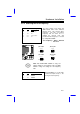
Hardware Installation 2.2.5 Clearing the CMOS JP14 1-2 2-3 Clear CMOS Normal operation (default) Clear CMOS You need to clear the CMOS if you forget your system password. To clear the CMOS, do the steps that follow the figure below. Before you proceed, check your onboard CMOS chip. The “clearing” procedures vary depending on the CMOS chip type. Read the CMOS chip label to determine the chip type. JP14 JP14 1 2 3 Normal Operation (default) 1 2 3 Clear CMOS For Dallas DS12887A: 1.
Hardware Installation For Dallas DS12B887, BENCHMARQ bq3287AMT, or SGS ST M48T86 PCI chip: 1. Turn off the system power. 2. Locate JP14 and short pins 2-3 for a few seconds. Check your manual for the correct jumper settings and location of the jumpers. 3. Turn on the system power. 4. Turn off the system power again. 5. Reset JP14 to its normal setting by shorting pins 1-2. 2.2.6 Selecting the DIMM Type JP25 Open 1-2 & 3-4 Memory Type SDRAM EDO JP25 lets you select your DIMM chip type.
Hardware Installation 2.3 Connectors 2.3.1 Power Cable A standard baby AT (PS/2) power supply has two cables with six wires on each cable. Plug in these cables to the onboard power connector in such a way that all the black wires are in the center. The power connector is marked PWR1 on the mainboard. Caution: Make sure that the power supply is OFF before connecting or disconnecting the power cable.
Hardware Installation 2.3.2 CPU Fan The fan connector is marked FAN on the system board. Plug in the fan cable to this 2-pin connector onboard. Attach the heatsink and fan to the CPU. Check its orientation, make sure the air flow go through the heatsink. +12V GND FAN Air Flow Heatsink 2.3.3 PS/2 Mouse Insert a PS/2 bracket connector to the connector marked PS2 MS on the mainboard. Then plug in the PS/2 mouse cable to the mouse port on the bracket.
Hardware Installation 2.3.4 Serial Devices (COM1/COM2) Plug in the 10-pin flat cable to the appropriate onboard connectors. The COM1 connector is marked COM1 and the COM2 connector is marked COM2 on the mainboard. Then insert the serial device connector into the serial port on the bracket.
Hardware Installation 2.3.5 USB Device (optional) You need a USB bracket to enable your system to support additional USB device(s). To attach a USB bracket, simply insert the bracket cable to the onboard connector marked USB.
Hardware Installation 2.3.6 Floppy Drive To support a floppy drive, connect the 34-pin floppy drive cable to the floppy drive connector marked FDC1 on the mainboard. 1 2 33 34 FDC1 2.3.7 Printer This connector allows you to install a printer to your system. To install, plug in the 26-pin printer flat cable to the onboard parallel connector marked PRINTER.
Hardware Installation 2.3.8 IDE Hard Disk and CD ROM This mainboard supports two 40-pin IDE connectors marked as IDE1 and IDE2. The IDE1 is also known as primary channel and IDE2 as secondary channel. Each channel supports two IDE devices. In order to enable the devices to work together, the two devices on each channel must be set differently to master and slave mode. The device can either be a hard disk or a CD-ROM. The setting of master or slave depends on your IDE device jumper.
Hardware Installation IDE1 (Primary Channel) Slave (2nd) Master (1st) IDE2 (Secondary Channel) Slave (4th) 2-22 Master (3rd)
Hardware Installation 2.3.9 Hard Disk LED The HDD LED connector is marked HDD LED on the board. This connector is designed to support various types of housing. Actually, only two pins are necessary for the LED. If your housing comes with a 4-pin connector, simply attach it to the onboard connector. For a 2-pin connector, you can insert it to pins 1-2 or pins 3-4. However, when connecting, take note of the polarity of the pins.
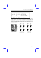
Hardware Installation 2.3.10 Panel Connector 1 The multifunction (panel) connector is a 20-pin connector marked PANEL on the board. Attach the power LED, keylock, speaker, reset switch, suspend switch, and green mode LED connectors to the corresponding pins as shown in the figure. Some housings come with a 5-pin connector for the keylock and power LED. Since the pins for power LED and keylock functions remained aligned, you can attach it to the onboard multifunction connector.
Hardware Installation Notes: If your housing comes with Turbo switch and Turbo LED connectors, you may use these connectors for Suspend switch and Green mode LED functions, respectively. Pressing the Suspend switch allows you to manually set the system to suspend mode. However, this is possible only if the Power Management function in the BIOS Setup menu is enabled.
Hardware Installation 2.3.11 Keyboard The onboard keyboard connector is a 5-pin AT-compatible connector marked KB1. The figure below shows how the keyboard connector as viewed from the back panel of the housing. Note: The mini DIN PS/2 keyboard connector is optional.
Hardware Installation 2.3.12 IrDA Connector Serial port 2 can be configured to support wireless infrared module via this connector and application software such as Laplink. This module enables the user to transfer files to or from laptops, notebooks, PDA and printers without using cables. This mainboard supports IrDA (115Kbps, 1 meter), as well as ASK-IR (19.2Kbps). To install an infrared module, insert the module cable to IrDA connector then enable infrared function by BIOS setup.
Hardware Installation 2.4 Configuring the System Memory Pin 1 of DIMM Pin 1 of Bank1 This mainboard has four 72 pin SIMM sockets (Single-in-line Memory Module) and one 168 pin DIMM socket (Dual-in-line Memory Module) that allow you to install system memory from minimum 8MB up to maximum 128MB. Pin 1 of Bank0 The SIMM supported by this mainboard can be identified by 4 kinds of factors, Intel VX chipset does not support 64M bit technology.
Hardware Installation II. Speed: normally marked as as -12, which means the clock cycle time is 12ns and maximum clock of this SDRAM is 83MHz. Sometimes you can also find the SDRAM marked as -67, which means maximum clock is 67MHz. III. Buffered and non-buffered: This motherboard supports non-buffered DIMMs.
Hardware Installation Warning: The default memory timing setting is 60ns to obtain the optimal performance. Because of the specification limitation, 70ns SIMM is recommended to be used only for CPU external clock 60MHz. Tip: EDO DRAM is designed to improve the DRAM read performance.
Hardware Installation For double side memory module, there is one limitation. This mainboard supports only 4 RAS# (Row address latch) signals for DRAM control. They can only be occupied by one DRAM module, they can not be shared. The simple rule is: If double side module at either Bank1 or DIMM, the other must be empty. Bank0 has no such limitation. Double side module at either Bank1 or DIMM socket, the other must be empty. Following table explains more about the RAS limitation.
Hardware Installation Warning: Do not use SIMM and SDRAM DIMM together unless you have 5V tolerance SDRAM (such as Samsung or TI). The FPM/EDO operate at 5V while SDRAM operates at 3.3V. If you combine them together the system will temporary work fine; however after a few months, the SDRAM 3.3V data input will be damaged by 5V FPM/EDO data output line. There is an important parameter affects SDRAM performance, CAS Latency Time.
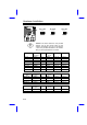
Hardware Installation Tip: The SIMM/DIMM chip count can be calculated by following example: 1. For 32 bit non-parity SIMM using 1M by 4 bit DRAM chip, 32/4=8 chips. 2. For 36 bit parity SIMM using 1M by 4 bit DRAM chip, 36/4=9 chips. 3. For 36 bit parity SIMM using 1M by 4 bit and 1M by 1 bit DRAM, the chip count will be 8 data chips(8= 32/4) plus 4 parity chips(4=4/1), total is 12 chips. 4. For 64 bit DIMM using 1M by 16 bit SDRAM, the chip count is 64/16=4 chips.
Hardware Installation DIMM Data chip 1M by 16 Bit size per side 1Mx64 Single/ Double side x1 Chip count 4 DIMM size Recommended 8MB Yes 1M by 16 1Mx64 x2 8 16MB Yes 2M by 8 2Mx64 x1 8 16MB Yes 2M by 8 2Mx64 x2 16 32MB Yes Tip: 8 bit = 1 byte, 32 bit = 4 byte. The SIMM size is represented by number of data byte (whether with or without parity), for example, the size of single side SIMM using 1M by 4 bit chip is 1Mx32 bit, that is, 1M x 4 byte = 4MB.