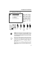
Chapter 2 Hardware Installation This chapter gives you a step-by-step procedure on how to install your system. Follow each section accordingly. Caution: Electrostatic discharge (ESD) can damage your processor, disk drives, expansion boards, and other components. Always observe the following precautions before you install a system component. 1. Do not remove a component from its protective packaging until you are ready to install it. 2.
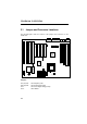
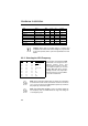
Hardware Installation 2.1 Jumper and Connector Locations The following figure shows the location of the jumpers and connectors on the mainboard.
Hardware Installation Connectors: PS2 MS: KB2: COM1: COM2: PRINTER: PWR2: USB: FDC: IDE1: IDE2: FAN1: FAN2: WKUP: IrDA: HDD LED: PANEL: PS/2 mouse connector PS/2 keyboard connector COM1 connector COM2 connector Printer connector ATX power connector USB connector Floppy drive connector IDE1 primary channel IDE2 secondary channel CPU fan connector (2-pin normal type) CPU fan connector (3-pin type for fan monitoring function) IR & MODEM wake-up connector IrDA (Infrared) connector HDD LED connector Front panel
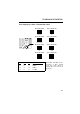
Hardware Installation 2.2 Jumpers Jumpers are made by pin headers and plastic connecting caps for the purpose of customizing your hardware. Doing so requires basic knowledge of computer hardware, be sure you understand the meaning of the jumpers before you change any setting. The onboard jumpers are normally set to their default with optimized settings. On the mainboard, normally there is a bold line marked beside pin 1 of the jumper, sometimes, there are numbers also.
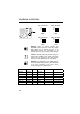
Hardware Installation 2.2.1 Setting the CPU Voltage JP11 1-2 3-4 5-6 7-8 9-10 11-12 CPU Core Voltage (Vcore) 3.45V (Intel P54C) 3.52V (Cyrix or AMD K5) 2.9V (AMD K6-166/200 or Cyrix M2) 2.8V (MMX P55C) 3.2V (AMD K6-233) 2.5V/2.2V/2.0V (Reserved) JP11 1 3 5 7 9 11 2 4 6 8 10 12 JP11 1 3 5 7 9 11 2 4 6 8 10 12 JP11 is used to select CPU core voltage (Vcore), normally it is set to default 3.45V for INTEL Pentium P54C.
Hardware Installation CPU Type JP11 Vcore Vio Vcpuio INTEL P54C Single Voltage 1-2 3.45V 3.45V Vcore INTEL MMX P55C Dual Voltage 7-8 2.8V 3.45V Vio AMD K5 Single Voltage 3-4 3.52V 3.45V Vcore AMD K6-166/200 Dual Voltage 5-6 2.9V 3.45V Vio AMD K6-233 Dual Voltage 9-10 3.2V 3.45V Vio Cyrix 6x86 Single Voltage 3-4 3.52V 3.45V Vcore Cyrix 6x86L Dual Voltage 7-8 2.8V 3.45V Vio Cyrix M2 Dual Voltage 5-6 2.9V 3.
Hardware Installation Core frequency = Ratio * External bus clock JP3 & JP2 & JP1 JP3 & JP2 & JP1 1 2 3 1 2 3 1.5x (3.5x) 2x JP3 & JP2 & JP1 JP3 & JP2 & JP1 1 2 3 1 2 3 2.5x (1.75x) 3x JP3 & JP2 & JP1 JP3 & JP2 & JP1 1 2 3 1 2 3 4x 4.5x JP3 & JP2 & JP1 JP3 & JP2 & JP1 1 2 3 5x JP4 1-2 2-3 2-3 1-2 JP5 2-3 2-3 1-2 1-2 JP6 1-2 1-2 1-2 2-3 CPU External Clock 60MHz 66MHz 75MHz 83.3MHz 1 2 3 5.
Hardware Installation JP4 & JP5 & JP6 JP4 & JP5 & JP6 JP6 JP5 JP4 JP6 JP5 JP4 1 2 3 1 2 3 60MHz 66MHz JP4 & JP5 & JP6 JP4 & JP5 & JP6 JP6 JP5 JP4 JP6 JP5 JP4 1 2 3 75MHz 1 2 3 83.3Mz Warning: INTEL TX chipset supports only 60/66MHz external CPU bus clock, the 75/83.3 MHz settings are for internal test only, set to 75/83.3MHz exceeds the specification of TX chipset, which may cause serious system damage. Caution: Following table are possible settings of current CPU available on the market.
Hardware Installation INTEL Pentium MMX CPU Core Frequency Ratio External Bus Clock JP1 & JP2 & JP3 JP4 & JP5 & JP6 PP/MT 150 150MHz = 2.5x 60MHz 2-3 & 2-3 & 1-2 1-2 & 2-3 & 1-2 PP/MT 166 166MHz = 2.5x 66MHz 2-3 & 2-3 & 1-2 2-3 & 2-3 & 1-2 PP/MT 200 200MHz = 3x 66MHz 1-2 & 2-3 & 1-2 2-3 & 2-3 & 1-2 PP/MT 233 233MHz = 3.
Hardware Installation Note: Cyrix 6x86, M2 and AMD K5 CPU use P-rating for the reference of CPU benchmark compared with INTEL P54C, their internal core frequency is not exactly equal to P-rating marked on the CPU. For example, Cyrix P166+ is 133MHz but performance is almost equal to P54C 166MHz and AMD PR133 is 100MHz but performance is almost equal to INTEL P54C 133MHz.
Hardware Installation 2.2.3 Clearing the CMOS JP14 1-2 2-3 Clear CMOS Normal operation (default) Clear CMOS You need to clear the CMOS if you forget your system password. To clear the CMOS, follow the procedures listed below: JP14 JP14 1 2 3 Normal Operation (default) 1 2 3 Clear CMOS The procedure to clear CMOS: 1. Turn off the system power. 2. Locate JP14 and short pins 2-3 for a few seconds. 3. Return JP14 to its normal setting by shorting pins 1-2. 4. Turn on the system power. 5.
Hardware Installation 2.3 Connectors 2.3.1 Power Cable The ATX power supply uses 20-pin connector shown below. Make sure you plug in the right direction. Caution: Make sure that the power supply is off before connecting or disconnecting the power cable. +5V 3.3V 5V SB 3.3V +5V PWR2 2.3.2 ATX Soft-Power Switch Connector The ATX soft-power switch connector is a 2-pin header on the system board. Locate the power switch cable from your ATX housing.
Hardware Installation 2.3.3 CPU Fan Plug in the fan cable to the 2-pin fan connector FAN1 or 3-pin FAN2 depends on the type of your fan. Three pins fan has an extra pin called SENSE, which periotically sends fan signal out. The fan monitoring function must use 3-pin fan. GND +12V SENSE FAN2 +12V GND FAN1 Air Flow Heatsink Attach the heatsink and fan to the CPU. Check its orientation, make sure the air flow go through the heatsink. 2.3.
Hardware Installation 2.3.5 Keyboard The onboard PS/2 keyboard connector is a 6-pin Mini-Din connector marked KB2. The view angle of drawing shown here is from back panel of the housing. PCB PS/2 KB 2.3.6 Serial Devices (COM1/COM2) The onboard serial connectors are 9-pin D-type connector on the back panel of mainboard. The serial port 1 connector is marked as COM1 and the serial port 2 connector is marked as COM2.
Hardware Installation 2.3.7 Printer The onboard printer connector is a 25-pin D-type connector marked PRINTER. The view angle of drawing shown here is from back panel of the housing. PCB PRINTER 2.3.8 USB Device You need a USB bracket to have your system to support additional USB device(s). To attach a USB bracket, simply insert the bracket cable to the onboard USB connector marked as USB. Pin 1 3 5 7 9 Description V0 D0D0+ GND NC Pin 2 4 6 8 10 Description V1 D1D1+ GND NC 2 1 9 10 USB 2.3.
Hardware Installation 2 34 1 33 FDC 2.3.10 IDE Hard Disk and CD ROM This mainboard supports two 40 pin IDE connectors marked as IDE1 and IDE2. IDE1 is also known as primary channel and IDE2 as secondary channel, each channel supports two IDE devices that makes total of four devices. In order to work together, the two devices on each channel must be set differently to master and slave mode, either one can be hard disk or CDROM.
Hardware Installation Caution: The specification of IDE cable is maximum 46cm (18 inches), make sure your cable does not excess this length. Caution: For better signal quality, it is recommended to set far end side device to master mode and follow the suggested sequence to install your new device . Please refer to following figure. IDE2 (Secondary Channel) Slave (4th) Master (3rd) IDE1 (Primary Channel) Slave (2nd) Master (1st) 2.3.
Hardware Installation + + + + 1 2 3 4 + + 1 2 3 4 1 2 3 4 HDD LED HDD LED HDD LED 4-pin connector 2-pin connector at pin 1-2 2-pin connector at pin 3-4 2.3.12 Panel Connector The Panel (multifunction) connector is a 20pin connector marked as PANEL on the board. Attach the power LED, keylock, speaker, reset switch, suspend switch, and green mode LED connectors to the corresponding pins as shown in the figure.
Hardware Installation Other housings may have a 12-pin connector. If your housing has this type of connector, connect it to PANEL as shown in the figure. Make sure that the red wire of the connector is connected to +5V. 1 11 +5V 10 20 PANEL Note: If your housing comes with Turbo switch and Turbo LED connectors, you may use these connectors for Suspend switch and Green mode LED functions, respectively. Caution:.
Hardware Installation 1 2 3 4 5 6 IrDA 2.3.14 Wake-up Connector This mainboard implements special circuit to support Modem Ring-On, both Internal Modem Card (AOpen MP32) and external box Modem are supported. Since Internal Modem card consumes no power when system power is off, it is recommended to use Internal Modem. To use AOpen MP32, connect 4-pin cable from RING connector of MP32 to WKUP connector on the mainboard. Refer to Appendix B "Frequently Asked Question" for detail.
Hardware Installation 2.4 Configuring the System Memory Pin 1 of DIMM2 Pin 1 of DIMM1 Pin 1 of Bank1 This mainboard has four 72 pin SIMM sockets (Single-in-line Memory Module) and two 168 pin DIMM socket (Dual-in-line Memory Module) that allow you to install system memory from minimum 8MB up to maximum 256MB.
Hardware Installation Warning: The default memory timing setting is 60ns to obtain the optimal performance. Because of the specification limitation, 70ns SIMM is recommended to be used only for CPU external clock 60MHz. Tip: EDO DRAM is designed to improve the DRAM read performance.
Hardware Installation For double side memory module, there is one limitation. This mainboard supports only 4 RAS# (Row address latch) signals for DRAM control. They can only be occupied by one DRAM module, they can not be shared. The simple rule is: If double side module at either Bank0 or DIMM1, the other must be empty, if you use double side at Bank0, DIMM1 must be empty. If you use at DIMM1, Bank0 must be empty. Bank1 and DIMM2 have the same limitation.
Hardware Installation Warning: Do not use SIMM and SDRAM DIMM together unless you have 5V tolerance SDRAM (such as Samsung or TI). The FPM/EDO operate at 5V while SDRAM operates at 3.3V. If you combine them together the system will temporary work fine; however after a few months, the SDRAM 3.3V data input will be damaged by 5V FPM/EDO data output line. There is an important parameter affects SDRAM performance, CAS Latency Time.
Hardware Installation Warning: Do not install any SIMM that contains more than 24 chips. SIMMs contain more than 24 chips exceed the INTEL chipset driving specification. Doing so may result in unstable system behavior. Warning: Although Intel TX chipset supports x4 SDRAM chip. Due to loading issue, it is not recommended to use this kind of SDRAM. Tip: The SIMM/DIMM chip count can be calculated by following example: 1. For 32 bit non-parity SIMM using 1M by 4 bit DRAM chip, 32/4=8 chips. 2.
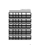
Hardware Installation SIMM Data chip SIMM Parity chip Bit size per side Single/ Double side Chip count SIMM size Recommended 16M by 4 None 16Mx32 x1 8 64MB Yes, but not tested. 16M by 4 None 16Mx32 x2 16 128MB Yes, but not tested. 16M by 4 16M by 4 16Mx36 x1 9 64MB Yes, but not tested. 16M by 4 16M by 4 16Mx36 x2 18 128MB Yes, but not tested.
Hardware Installation Following table are possible DRAM combinations that is NOT recommended: SIMM Data chip SIMM Parity chip Bit size per side Single/ Double side Chip count SIMM size Recommended 1M by 1 None 1Mx32 x1 32 4MB No 1M by 1 1M by 1 1Mx36 x1 36 4MB No 1M by 4 1M by 1 1Mx36 x2 24 8MB No 4M by 1 None 4Mx32 x1 32 16MB No 4M by 1 4M by 1 4Mx36 x1 36 16MB No 16M by 1 None 16Mx32 x1 32 64MB No 16M by 1 16M by 1 16Mx36 x1 36 64MB No DIMM Data chip