
User's Manual


PRELIMINARY DATA SHEET • SKY85717-21: FRONT-END MODULE
Skyworks Solutions, Inc. • Phone [781] 376-3000 • Fax [781] 376-3100 • sales@skyworksinc.com • www.skyworksinc.com
6 August 18, 2014 • Skyworks Proprietary Information • Products and Product Information are Subject to Change Without Notice • 203068E
Evaluation Board Description
The SKY85717-21 Evaluation Board is used to test the
performance of the SKY85717-21 FEM. A suggested application
schematic diagram is shown in Figure 3. A photograph of the
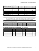
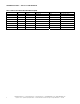
Evaluation Board is shown in Figure 4. A Bill of Materials (BOM)
for the Evaluation Board is provided in Table 8.
Evaluation Board Test Procedures
1. Connect the system ground to connector J4, pin 2, of the
Evaluation Board.
2. Apply 5 V to connector J4, pins 1 and 3.
3. Select a path to test according to the modes shown in
Table 7.
4. Connect a multimeter or oscilloscope to connector J5, pin 12,
to monitor the power detector voltage.
5. Apply an RF signal to connector J1 (ANT) to monitor the RX to
ANT performance. Measure the response from the output of
connector J2 (RX).
6. Apply an RF signal to connector J3 (TX) to monitor the ANT to
TX performance. Monitor the output power on connector J1
(ANT). Care should be taken not to overdrive the amplifier by
applying too much RF on the input to the device (–20 dBm
provides a suitable starting input power for the device).
9BCircuit Design Considerations
The following design considerations are general in nature and
must be followed regardless of final use or configuration:
Paths to ground should be made as short as possible.
The RX and ANT ports are AC-coupled and do not require DC
blocking capacitors. There are ESD diodes to ground and a DC
blocking capacitor between the TX port (pin 8) and the die.
Therefore, there is no DC present on this port.
If the TX port is connected to an external component with
>3 VDC present on it, a 10 pF (component C8) general
purpose blocking capacitor is recommended.
Capacitors C6 (1 μF) and C7 (100 pF) should be on the
primary side of the Evaluation Board at a minimum
manufacturable distance from the FEM.
Capacitor C20 (0.3 pF) needs to be as close as possible at
manufacturable distance from the ANT pin of the IC, followed
by L1 (1.0 nH) and C19 (0.3 pF), also at manufacturable
distance from C20 and L1, respectively.
The ground pad of the SKY85717-21 has special electrical
and thermal grounding requirements. This pad is the main
thermal conduit for heat dissipation. Because the circuit board
acts as the heat sink, it must shunt as much heat as possible
from the device. Therefore, design the connection to the
ground pad to dissipate the maximum wattage produced by
the circuit board. Multiple vias to the grounding layer are
required.
Evaluation Board trace losses are:
RX = TX = 0.32 dB and ANT = 0.35 dB.
NOTE: A poor connection between the ground pad and the
ground increases the junction temperature (T
J), which
reduces the life of the device.
Package Dimensions
The PCB layout footprint for the SKY85717-21 is shown in
Figure 5. Typical part markings are shown in Figure 6. Package
dimensions for the 16-pin QFN are shown in Figure 7, and tape
and reel dimensions are provided in Figure 8.