
Datasheet

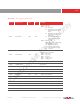
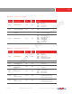

Table Of Contents
- applications
- features
- key specifications
- table of contents
- list of figures
- list of tables
- 1 signal descriptions
- 2 system level description
- 3 block level description
- 4 image sensor core digital functions
- 4.1 mirror and flip
- 4.2 image windowing
- 4.3 test pattern
- 4.4 50/60Hz detection
- 4.5 AEC and AGC algorithms
- 4.6 AEC/AGC steps
- 4.7 black level calibration (BLC)
- 4.8 strobe flash and frame exposure
- 4.9 xenon flash control
- 4.10 frame exposure (FREX) mode
- 4.11 FREX strobe flash control
- 4.12 one-time programmable (OTP) memory
- 5 image sensor processor digital functions
- 6 image sensor output interface digital functions
- 7 register tables
- table 7-1 system control registers (sheet 1 of 5)
- table 7-2 SCCB registers (sheet 1 of 2)
- table 7-3 group hold control registers
- table 7-4 AEC/AGC 1 registers
- table 7-5 system timing registers (sheet 1 of 3)
- table 7-6 AEC/AGC 2 registers (sheet 1 of 3)
- table 7-7 STROBE/frame exposure control registers (sheet 1 of 2)
- table 7-8 50/60 HZ DETECTION registers
- table 7-9 OTP control registers (sheet 1 of 2)
- table 7-10 BLC registers (sheet 1 of 3)
- table 7-11 frame control registers
- table 7-12 DVP registers (sheet 1 of 2)
- table 7-13 MIPI top registers (sheet 1 of 11)
- table 7-14 ISPFC registers
- table 7-15 ISP TOP control registers (sheet 1 of 6)
- table 7-16 AWB registers (sheet 1 of 3)
- table 7-17 average registers (sheet 1 of 2)
- table 7-18 DPC registers
- table 7-19 LENC registers (sheet 1 of 4)
- table 7-20 cluster DPC registers (sheet 1 of 2)
- table 7-21 windows registers
- table 7-22 AEC/AGC 3 registers
- 8 operating specifications
- 9 mechanical specifications
- 10 optical specifications
- revision history

Confidential for truly Only
color CMOS QSXGA (5 megapixel) image sensor with OmniBSI™ technology
OV5647
proprietary to OmniVision Technologies PRELIMINARY SPECIFICATION version 1.0
0x4801 MIPI CTRL 01 0x0F RW
MIPI Control 01
Bit[7]: Long packet data type manual enable
0: Use mipi_dt
1: Use dt_man_o as long packet
data
(see register 0x4814[5:0])
Bit[6]: Short packet data type manual enable
1: Use dt_spkt as short packet data
(see register 0x4815[5:0])
Bit[5]: Short packet WORD COUNTER
manual enable
0: Use frame counter or line counter
1: Select spkt_wc_reg_o
(see {0x4812, 0x4813})
Bit[4]: PH bit order for ECC
0: {DI[7:0],WC[7:0],WC[15:8]}
1: {DI[0:7],WC[0:7],WC[8:15]}
Bit[3]: PH byte order for ECC
0: {DI,WC_l,WC_h}
1: {DI,WC_h,WC_l}
Bit[2]: PH byte order2 for ECC
0: {DI,WC}
1: {WC,DI}
Bit[1]: mark1_en1
0: Not used
1: After each rst release, lane 1
should send mark1 for
wkup_dly_o when mipi_sys_susp
=1
Bit[0]: mark1_en2
0: Not used
1: After each reset release, lane 2
should send mark1 for
wkup_dly_o when
mipi_sys_susp=1
table 7-13 MIPI top registers (sheet 2 of 11)
address
register name
default
value
R/W
description