
Datasheet
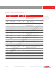
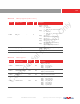
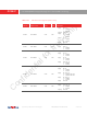
Table Of Contents
- applications
- features
- key specifications
- table of contents
- list of figures
- list of tables
- 1 signal descriptions
- 2 system level description
- 3 block level description
- 4 image sensor core digital functions
- 4.1 mirror and flip
- 4.2 image windowing
- 4.3 test pattern
- 4.4 50/60Hz detection
- 4.5 AEC and AGC algorithms
- 4.6 AEC/AGC steps
- 4.7 black level calibration (BLC)
- 4.8 strobe flash and frame exposure
- 4.9 xenon flash control
- 4.10 frame exposure (FREX) mode
- 4.11 FREX strobe flash control
- 4.12 one-time programmable (OTP) memory
- 5 image sensor processor digital functions
- 6 image sensor output interface digital functions
- 7 register tables
- table 7-1 system control registers (sheet 1 of 5)
- table 7-2 SCCB registers (sheet 1 of 2)
- table 7-3 group hold control registers
- table 7-4 AEC/AGC 1 registers
- table 7-5 system timing registers (sheet 1 of 3)
- table 7-6 AEC/AGC 2 registers (sheet 1 of 3)
- table 7-7 STROBE/frame exposure control registers (sheet 1 of 2)
- table 7-8 50/60 HZ DETECTION registers
- table 7-9 OTP control registers (sheet 1 of 2)
- table 7-10 BLC registers (sheet 1 of 3)
- table 7-11 frame control registers
- table 7-12 DVP registers (sheet 1 of 2)
- table 7-13 MIPI top registers (sheet 1 of 11)
- table 7-14 ISPFC registers
- table 7-15 ISP TOP control registers (sheet 1 of 6)
- table 7-16 AWB registers (sheet 1 of 3)
- table 7-17 average registers (sheet 1 of 2)
- table 7-18 DPC registers
- table 7-19 LENC registers (sheet 1 of 4)
- table 7-20 cluster DPC registers (sheet 1 of 2)
- table 7-21 windows registers
- table 7-22 AEC/AGC 3 registers
- 8 operating specifications
- 9 mechanical specifications
- 10 optical specifications
- revision history

Confidential for truly Only
color CMOS QSXGA (5 megapixel) image sensor with OmniBSI™ technology
OV5647
proprietary to OmniVision Technologies PRELIMINARY SPECIFICATION version 1.0
0x4819 HS_ZERO_MIN 0x96 RW
Low byte of the minimum value for hs_zero, unit ns
hs_zero_real = hs_zero_min_o +
Tui*ui_hs_zero_min_o
0x481A HS_TRAIL_MIN 0x00 RW High byte of the minimum value for hs_trail, unit ns
0x481B HS_TRAIL_MIN 0x3C RW
Low byte of the minimum value for hs_trail,
hs_trail_real = hs_trail_min_o +
Tui*ui_hs_trail_min_o
0x481C CLK_ZERO_MIN 0x01 RW
High byte of the minimum value for clk_zero
Unit ns
0x481D CLK_ZERO_MIN 0x86 RW
Low byte of the minimum value for clk_zero,
clk_zero_real = clk_zero_min_o +
Tui*ui_clk_zero_min_o
0x481E
CLK_PREPARE_
MIN
0x00 RW
High byte of the minimum value for clk_prepare,
Unit ns
Bit[7:2]: Not used
Bit[1:0]: clk_prepare_min[9:8]
0x481F
CLK_PREPARE_
MIN
0x3C RW
Low byte of the minimum value for clk_prepare
clk_prepare_real = clk_prepare_min_o +
Tui*ui_clk_prepare_min_o
0x4820 CLK_POST_MIN 0x00 RW
High byte of the minimum value for clk_post
Unit ns
Bit[7:2]: Not used
Bit[1:0]: clk_post_min[9:8]
0x4821 CLK_POST_MIN 0x56 RW
Low byte of the minimum value for clk_post
clk_post_real = clk_post_min_o +
Tui*ui_clk_post_min_o
0x4822 CLK_TRAIL_MIN 0x00 RW
High byte of the minimum value for clk_trail, unit ns
Bit[7:2]: Not used
Bit[1:0]: clk_trail_min[9:8]
0x4823 CLK_TRAIL_MIN 0x3C RW
Low byte of the minimum value for clk_trail
clk_trail_real = clk_trail_min_o +
Tui*ui_clk_trail_min_o
0x4824 LPX_P_MIN 0x00 RW
High byte of the minimum value for lpx_p, unit ns
Bit[7:2]: Not used
Bit[1:0]: lpx_p_min[9:8]
0x4825 LPX_P_MIN 0x32 RW
Low byte of the minimum value for lpx_p
lpx_p_real = lpx_p_min_o + Tui*ui_lpx_p_min_o
0x4826 HS_PREPARE_MIN 0x00 RW
High byte of the minimum value for hs_prepare,
unit ns
Bit[7:2]: Not used
Bit[1:0]: hs_prepare_min[9:8]
table 7-13 MIPI top registers (sheet 8 of 11)
address
register name
default
value
R/W
description