
Datasheet
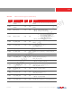
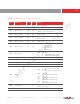


Table Of Contents
- applications
- features
- key specifications
- table of contents
- list of figures
- list of tables
- 1 signal descriptions
- 2 system level description
- 3 block level description
- 4 image sensor core digital functions
- 4.1 mirror and flip
- 4.2 image windowing
- 4.3 test pattern
- 4.4 50/60Hz detection
- 4.5 AEC and AGC algorithms
- 4.6 AEC/AGC steps
- 4.7 black level calibration (BLC)
- 4.8 strobe flash and frame exposure
- 4.9 xenon flash control
- 4.10 frame exposure (FREX) mode
- 4.11 FREX strobe flash control
- 4.12 one-time programmable (OTP) memory
- 5 image sensor processor digital functions
- 6 image sensor output interface digital functions
- 7 register tables
- table 7-1 system control registers (sheet 1 of 5)
- table 7-2 SCCB registers (sheet 1 of 2)
- table 7-3 group hold control registers
- table 7-4 AEC/AGC 1 registers
- table 7-5 system timing registers (sheet 1 of 3)
- table 7-6 AEC/AGC 2 registers (sheet 1 of 3)
- table 7-7 STROBE/frame exposure control registers (sheet 1 of 2)
- table 7-8 50/60 HZ DETECTION registers
- table 7-9 OTP control registers (sheet 1 of 2)
- table 7-10 BLC registers (sheet 1 of 3)
- table 7-11 frame control registers
- table 7-12 DVP registers (sheet 1 of 2)
- table 7-13 MIPI top registers (sheet 1 of 11)
- table 7-14 ISPFC registers
- table 7-15 ISP TOP control registers (sheet 1 of 6)
- table 7-16 AWB registers (sheet 1 of 3)
- table 7-17 average registers (sheet 1 of 2)
- table 7-18 DPC registers
- table 7-19 LENC registers (sheet 1 of 4)
- table 7-20 cluster DPC registers (sheet 1 of 2)
- table 7-21 windows registers
- table 7-22 AEC/AGC 3 registers
- 8 operating specifications
- 9 mechanical specifications
- 10 optical specifications
- revision history

Confidential for truly Only
11.03.2009 PRELIMINARY SPECIFICATION proprietary to OmniVision Technologies
6-17
0x4804 MIPI CTRL 04 0x8D RW
MIPI Control 04
Bit[7]: wait_pkt_end
1: Wait HS packet end when send UL
command
Bit[6]: tx_lsb_first
0: lp_tx and lp_rx high bit first
1: Low power transmit low bit first
Bit[5]: dir_recover_sel
0: Auto change to output only when
TurnAround command
1: Auto change to output when LP11
and GPIO is output
Bit[4]: mipi_reg_en
0: Disable MIPI_REG_P to access
registers, LP data will write to VFIFO
1: Enable MIPI_REG_P to access
registers
Bit[3]: Address read/write register will auto add 1
0: Disable
1: Enable
Bit[2]: LP TX lane select
0: Select lane1 to transmit LP data
1: Select lane2 to transmit LP data
Bit[1]: wr_first_byte
1: lp_rx will write first byte (command
byte) to RAM
Bit[0]: rd_ta_en
1: Send TurnAround command after
sending register read data
table 6-9 MIPI transmitter registers (sheet 4 of 8)
address
register name
default
value
R/W
description