
Datasheet
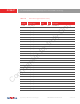

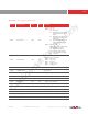
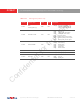
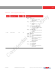

Table Of Contents
- applications
- features
- key specifications
- table of contents
- list of figures
- list of tables
- 1 signal descriptions
- 2 system level description
- 3 block level description
- 4 image sensor core digital functions
- 4.1 mirror and flip
- 4.2 image windowing
- 4.3 test pattern
- 4.4 50/60Hz detection
- 4.5 AEC and AGC algorithms
- 4.6 AEC/AGC steps
- 4.7 black level calibration (BLC)
- 4.8 strobe flash and frame exposure
- 4.9 xenon flash control
- 4.10 frame exposure (FREX) mode
- 4.11 FREX strobe flash control
- 4.12 one-time programmable (OTP) memory
- 5 image sensor processor digital functions
- 6 image sensor output interface digital functions
- 7 register tables
- table 7-1 system control registers (sheet 1 of 5)
- table 7-2 SCCB registers (sheet 1 of 2)
- table 7-3 group hold control registers
- table 7-4 AEC/AGC 1 registers
- table 7-5 system timing registers (sheet 1 of 3)
- table 7-6 AEC/AGC 2 registers (sheet 1 of 3)
- table 7-7 STROBE/frame exposure control registers (sheet 1 of 2)
- table 7-8 50/60 HZ DETECTION registers
- table 7-9 OTP control registers (sheet 1 of 2)
- table 7-10 BLC registers (sheet 1 of 3)
- table 7-11 frame control registers
- table 7-12 DVP registers (sheet 1 of 2)
- table 7-13 MIPI top registers (sheet 1 of 11)
- table 7-14 ISPFC registers
- table 7-15 ISP TOP control registers (sheet 1 of 6)
- table 7-16 AWB registers (sheet 1 of 3)
- table 7-17 average registers (sheet 1 of 2)
- table 7-18 DPC registers
- table 7-19 LENC registers (sheet 1 of 4)
- table 7-20 cluster DPC registers (sheet 1 of 2)
- table 7-21 windows registers
- table 7-22 AEC/AGC 3 registers
- 8 operating specifications
- 9 mechanical specifications
- 10 optical specifications
- revision history

Confidential for truly Only
11.03.2009 PRELIMINARY SPECIFICATION proprietary to OmniVision Technologies
7-21
table 7-11 frame control registers
address
register name
default
value
R/W
description
0x4200 FRAME CTRL0 0x00 RW
Bit[7:3]: Not used
Bit[2]: fcnt_eof_sel
Bit[1]: fcnt_mask_dis
Bit[0]: fcnt_reset
0x4201 FRAME ON NUMBER 0x00 RW
Bit[7:4]: Not used
Bit[3:0]: Frame ON number
0x4202
FRAME OFF
NUMBER
0x00 RW
Bit[7:4]: Not used
Bit[3:0]: Frame OFF number
0x4203 FRAME CTRL1 0x00 RW
Bit[7:6]: Not used
Bit[5]: data_mask_dis
Bit[4]: valid_mask_dis
Bit[3]: href_mask_dis
Bit[2]: eof_mask_dis
Bit[1]: sof_mask_dis
Bit[0]: all_mask_dis
table 7-12 DVP registers (sheet 1 of 2)
address
register name
default
value
R/W
description
0x4700 MODE SELECT 0x04 RW
Bit[7:4]: Not used
Bit[3]: CCIR V select
Bit[2]: CCIR F select
Bit[1]: CCIR656 mode enable
Bit[0]: HSYNC mode enable
0x4701 VSYNC WIDTH 0x01 RW VSYNC Length in Terms of Line Count
0x4702
VSYNC
NEG_WIDTH_H
0x01 RW
Bit[7:0]: VSYNC length in terms of pixel
count[15:8]
0x4703
VSYNC
NEG_WIDTH_L
0x00 RW
Bit[7:0]: VSYNC length in terms of pixel
count[7:0]
0x4704 VSYNC MODE 0x00 RW
Bit[7:4]: Not used
Bit[3:2]: r_vsyncout_sel
Bit[1]: VSYNC mode3
Bit[0]: VSYNC mode2
0x4705
EOF
VSYNC_DELAY_2
0x00 RW
Bit[7:0]: eof_vsync_delay[23:16]
SOF/EOF negative edge to
VSYNC positive edge delay
0x4706
EOF
VSYNC_DELAY_1
0x00 RW
Bit[7:0]: eof_vsync_delay[15:8]
SOF/EOF negative edge to
VSYNC positive edge dealy