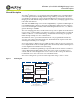
MT9V022: 1/3-Inch Wide-VGA Digital Image Sensor Features 1/3-Inch Wide-VGA CMOS Digital Image Sensor MT9V022 For the latest data sheet revision, refer to Aptina’s Web site: www.aptina.
MT9V022: 1/3-Inch Wide-VGA Digital Image Sensor Table of Contents Table of Contents Features . . . . . . . . . . . . . . . . . . . . . . . . . . . . . . . . . . . . . . . . . . . . . . . . . . . . . . . . . . . . . . . . . . . . . . . . . . . . . . . . . . . . . . . . . . . . . .1 Applications . . . . . . . . . . . . . . . . . . . . . . . . . . . . . . . . . . . . . . . . . . . . . . . . . . . . . . . . . . . . . . . . . . . . . . . . . . . . . . . . . . . . . . . . . .1 Ordering Information. . . . . . . .
MT9V022: 1/3-Inch Wide-VGA Digital Image Sensor Table of Contents Gain Settings . . . . . . . . . . . . . . . . . . . . . . . . . . . . . . . . . . . . . . . . . . . . . . . . . . . . . . . . . . . . . . . . . . . . . . . . . . . . . . . . . . . . . .28 Changes to Gain Settings . . . . . . . . . . . . . . . . . . . . . . . . . . . . . . . . . . . . . . . . . . . . . . . . . . . . . . . . . . . . . . . . . . . . . . . . .28 Digital Gain . . . . . . . . . . . . . . . . . . . . . . . . . . . . . . . . . . . .
MT9V022: 1/3-Inch Wide-VGA Digital Image Sensor List of Figures List of Figures Figure 1: Figure 2: Figure 3: Figure 4: Figure 5: Figure 6: Figure 7: Figure 8: Figure 9: Figure 10: Figure 11: Figure 12: Figure 13: Figure 14: Figure 15: Figure 16: Figure 17: Figure 18: Figure 19: Figure 20: Figure 21: Figure 22: Figure 23: Figure 24: Figure 25: Figure 26: Figure 27: Figure 28: Figure 29: Figure 30: Figure 31: Figure 32: Figure 33: Figure 34: Figure 35: Figure 36: Figure 37: Figure 38: Figure 39: Figure 40: F
MT9V022: 1/3-Inch Wide-VGA Digital Image Sensor List of Tables List of Tables Table 1: Table 2: Table 3: Table 4: Table 5: Table 6: Table 7: Table 8: Table 9: Table 10: Table 11: Table 12: Table 13: Key Performance Parameters. . . . . . . . . . . . . . . . . . . . . . . . . . . . . . . . . . . . . . . . . . . . . . . . . . . . . . . . . . . . . . .1 Available Part Numbers. . . . . . . . . . . . . . . . . . . . . . . . . . . . . . . . . . . . . . . . . . . . . . . . . . . . . . . . . . . . . . . . . . . .
MT9V022: 1/3-Inch Wide-VGA Digital Image Sensor General Description General Description The Aptina® MT9V022 is a 1/3-inch wide-VGA format CMOS active-pixel digital image sensor with global shutter and high dynamic range (HDR) operation. The sensor has specifically been designed to support the demanding interior and exterior automotive imaging needs, which makes this part ideal for a wide variety of imaging applications in real-world environments.
MT9V022: 1/3-Inch Wide-VGA Digital Image Sensor General Description Figure 2: 52-Ball IBGA Package 1 2 3 4 5 A VDD LVDS SER_ DATAOUT _P SER_ DATAOUT _N VDD LVDS SYSCLK B LVDS GND SHFT_ CLKOUT _P SHFT_ CLKOUT _N VDD C BYPASS _CLKIN _P BYPASS _CLKIN _N LVDS GND D SER_ DATAIN _P E 6 7 8 DOUT2 DOUT3 DOUT1 DOUT4 VAAPIX DGND AGND VAA SER_ DATAIN _N NC NC DOUT5 VDD NC NC F DOUT6 DOUT7 DGND AGND VAA STANDBY G DOUT8 FRAME _VALID STLN_ OUT SDATA STFRM_ OUT LED_
MT9V022: 1/3-Inch Wide-VGA Digital Image Sensor Ball Descriptions Ball Descriptions Table 3: Ball Descriptions Only pins DOUT0 through DOUT9 may be tri-stated.
MT9V022: 1/3-Inch Wide-VGA Digital Image Sensor Ball Descriptions Table 3: Ball Descriptions (continued) Only pins DOUT0 through DOUT9 may be tri-stated. 52-Ball IBGA Numbers Symbol Type A2 B4, E2 C8, F7 B8 A1, A4 B1, C3 C6, F3 C7, F6 E7, E8, D7, D8 SER_DATAOUT_P VDD VAA VAAPIX VDDLVDS LVDSGND DGND AGND NC Output Supply Supply Supply Supply Ground Ground Ground NC Notes: Figure 3: Description Note Serial data out (differential positive). Digital power 3.3V. Analog power 3.3V. Pixel power 3.3V.
MT9V022: 1/3-Inch Wide-VGA Digital Image Sensor Pixel Data Format Pixel Data Format Pixel Array Structure The MT9V022 pixel array is configured as 782 columns by 492 rows, shown in Figure 4. The left 26 columns and the top eight rows of pixels are optically black and can be used to monitor the black level. The black row data is used internally for the automatic black level adjustment. However, the middle four black rows can also be read out by setting the sensor to raw data output mode.
MT9V022: 1/3-Inch Wide-VGA Digital Image Sensor Color Device Limitations Color Device Limitations The color version of the MT9V022 does not support or offers reduced performance for the following functionalities. Pixel Binning Pixel binning is done on immediate neighbor pixels only, no facility is provided to skip pixels according to a Bayer pattern. Therefore, the result of binning combines pixels of different colors. For more information, see “Pixel Binning” on page 34.
MT9V022: 1/3-Inch Wide-VGA Digital Image Sensor Output Data Format Figure 6: Spatial Illustration of Image Readout P0,0 P0,1 P0,2.....................................P0,n-1 P0,n P1,0 P1,1 P1,2.....................................P1,n-1 P1,n VALID IMAGE HORIZONTAL BLANKING Pm-1,0 Pm-1,1.....................................Pm-1,n-1 Pm-1,n Pm,0 Pm,1.....................................Pm,n-1 Pm,n 00 00 00 .................. 00 00 00 00 00 00 .................. 00 00 00 00 00 00 .........................
MT9V022: 1/3-Inch Wide-VGA Digital Image Sensor Output Data Format Output Data Timing The data output of the MT9V022 is synchronized with the PIXCLK output. When LINE_VALID is HIGH, one 10-bit pixel datum is output every PIXCLK period. Figure 7: Timing Example of Pixel Data ... LINE_VALID ... PIXCLK Blanking P0 (9:0) DOUT(9:0) ... Valid Image Data P1 (9:0) P2 (9:0) P3 (9:0) P4 (9:0) ... Blanking Pn-1 (9:0) Pn (9:0) The PIXCLK is a nominally inverted version of the master clock (SYSCLK).
MT9V022: 1/3-Inch Wide-VGA Digital Image Sensor Output Data Format Table 4: Frame Time (continued) Parameter Name Equation Default Timing at 26.66 MHz A+Q Row time R0x04 + R0x05 V Vertical blanking (R0x06) x (A + Q) + 4 Nrows x (A + Q) Frame valid time (R0x03) × (A + Q) F Total frame time V + (Nrows x (A + Q)) 846 pixel clocks = 846 master = 31.72μs 38,074 pixel clocks = 38,074 master = 1.43ms 406,080 pixel clocks = 406,080 master = 15.23ms 444,154 pixel clocks = 444,154 master = 16.
MT9V022: 1/3-Inch Wide-VGA Digital Image Sensor Serial Bus Description Serial Bus Description Registers are written to and read from the MT9V022 through the two-wire serial interface bus. The MT9V022 is a serial interface slave with four possible IDs (0x90, 0x98, 0xB0 and 0xB8) determined by the S_CTRL_ADR0 and S_CTRL_ADR1 input pins. Data is transferred into the MT9V022 and out through the serial data (SDATA) line. The SDATA line is pulled up to VDD off-chip by a 1.5KΩ resistor.
MT9V022: 1/3-Inch Wide-VGA Digital Image Sensor Serial Bus Description Start Bit The start bit is defined as a HIGH-to-LOW transition of the data line while the clock line is HIGH. Stop Bit The stop bit is defined as a LOW-to-HIGH transition of the data line while the clock line is HIGH. Slave Address The 8-bit address of a two-wire serial interface device consists of 7 bits of address and 1 bit of direction. A “0” in the LSB of the address indicates write mode, and a “1” indicates read mode.
MT9V022: 1/3-Inch Wide-VGA Digital Image Sensor Two-Wire Serial Interface Sample Read and Write Sequences Two-Wire Serial Interface Sample Read and Write Sequences 16-Bit Write Sequence A typical write sequence for writing 16 bits to a register is shown in Figure 9. A start bit given by the master, followed by the write address, starts the sequence. The image sensor then gives an acknowledge bit and expects the register address to come first, followed by the 16-bit data.
MT9V022: 1/3-Inch Wide-VGA Digital Image Sensor Two-Wire Serial Interface Sample Read and Write Sequences 8-Bit Write Sequence To be able to write 1 byte at a time to the register a special register address is added. The 8-bit write is done by first writing the upper 8 bits to the desired register and then writing the lower 8 bits to the special register address (R0xF0). The register is not updated until all 16 bits have been written. It is not possible to just update half of a register.
MT9V022: 1/3-Inch Wide-VGA Digital Image Sensor Two-Wire Serial Interface Sample Read and Write Sequences Register Lock Included in the MT9V022 is a register lock (R0xFE) feature that can be used as a solution to reduce the probability of an inadvertent noise-triggered two-wire serial interface write to the sensor.
MT9V022: 1/3-Inch Wide-VGA Digital Image Sensor Feature Description Feature Description Operational Modes The MT9V022 works in master, snapshot, or slave mode. In master mode the sensor generates the readout timing. In snapshot mode it accepts an external trigger to start integration, then generates the readout timing. In slave mode the sensor accepts both external integration and readout controls.
MT9V022: 1/3-Inch Wide-VGA Digital Image Sensor Feature Description When exposure time is greater than the sum of vertical blank and window height, the number of vertical blank rows is increased automatically to accommodate the exposure time. Sequential Master Mode In sequential master mode the exposure period is followed by readout. The frame synchronization waveforms for sequential master mode are shown in Figure 15. The frame rate changes as the integration time changes.
MT9V022: 1/3-Inch Wide-VGA Digital Image Sensor Feature Description Figure 17: Snapshot Mode Frame Synchronization Waveforms EXPOSURE Exposure Time LED_OUT FRAME_VALID LINE_VALID DOUT(9:0) xxx xxx xxx Slave Mode In slave mode, the exposure and readout are controlled using the EXPOSURE, STFRM_OUT, and STLN_OUT pins. When the slave mode is enabled, STFRM_OUT and STLN_OUT become input pins. The start and end of integration are controlled by EXPOSURE and STFRM_OUT pulses, respectively.
MT9V022: 1/3-Inch Wide-VGA Digital Image Sensor Feature Description Signal Path The MT9V022 signal path consists of a programmable gain, a programmable analog offset, and a 10-bit ADC. See “Black Level Calibration” on page 30 for the programmable offset operation description.
MT9V022: 1/3-Inch Wide-VGA Digital Image Sensor Feature Description Window Control Registers R0x01 column start, R0x02 Row Start, R0x03 window height (row size), and R0x04 Window Width (column size) control the size and starting coordinates of the window. The values programmed in the window height and width registers are the exact window height and width out of the sensor. The window start value should never be set below four. To read out the dark rows set bit 6 of R0x0D.
MT9V022: 1/3-Inch Wide-VGA Digital Image Sensor Feature Description Changes to Integration Time With automatic exposure control disabled (R0xAF, bit 0 is cleared to LOW), and if the total integration time (R0x0B) is changed via the two-wire serial interface while FRAME_VALID is asserted for frame n, the first frame output using the new integration time is frame (n + 2).
MT9V022: 1/3-Inch Wide-VGA Digital Image Sensor Feature Description Exposure Indicator The exposure indicator is controlled by: • R0x1B LED_OUT Control The MT9V022 provides an output pin, LED_OUT, to indicate when the exposure takes place. When R0x1B bit 0 is clear, LED_OUT is HIGH during exposure. By using R0x1B, bit 1, the polarity of the LED_OUT pin can be inverted.
MT9V022: 1/3-Inch Wide-VGA Digital Image Sensor Feature Description The parameters of the step voltage V_Step which takes values V1, V2, and V3 directly affect the position of the knee points in Figure 22. Light intensities work approximately as a reciprocal of the partial exposure time. Typically, t1 is the longest exposure, t2 shorter, and so on. Thus the range of light intensities is shortest for the first slope, providing the highest sensitivity.
MT9V022: 1/3-Inch Wide-VGA Digital Image Sensor Feature Description Figure 23: 12- to 10-Bit Companding Chart 10-bit Codes 1,024 768 8 to 1 Companding (2,048 4 to 1 Companding (1,536 512 2 to 1 Companding (256 256 No companding (256 256 512 1,024 256) 384) 128) 12-bit Codes 256) 2,048 4,096 Gain Settings Changes to Gain Settings When the digital gain settings (R0x80–R0x98) are changed, the gain is updated on the next frame start.
MT9V022: 1/3-Inch Wide-VGA Digital Image Sensor Feature Description Analog Gain Analog gain is controlled by: • R0x35 Global Gain The formula for gain setting is: Gain = Bits[6:0] x 0.0625 (EQ 7) The analog gain range supported in the MT9V022 is 1X–4X with a step size of 6.25 percent. To control gain manually with this register, the sensor must NOT be in AGC mode.
MT9V022: 1/3-Inch Wide-VGA Digital Image Sensor Feature Description Registers 0x99–0x9E and 0x9F–0xA4 represent the coordinates X0/5-X5/5 and Y0/5-Y5/5 in Figure 25, respectively. Digital gains of registers 0x80–0x98 apply to their corresponding tiles. The MT9V022 supports a digital gain of 0.25-3.75X. The formula for digital gain setting is: Digital Gain = Bits[3:0] x 0.
MT9V022: 1/3-Inch Wide-VGA Digital Image Sensor Feature Description In normal operation, the black level calibration value/offset correction value is calculated at the beginning of each frame and can be read through the two-wire serial interface from R0x48. This register is an 8-bit signed two’s complement value. However, if R0x47, bit 0 is set to “1,” the calibration value in R0x48 may be manually set to override the automatic black level calculation result.
MT9V022: 1/3-Inch Wide-VGA Digital Image Sensor Feature Description Automatic Gain Control and Automatic Exposure Control The integrated AEC/AGC unit is responsible for ensuring that optimal auto settings of exposure and (analog) gain are computed and updated every frame. AEC and AGC can be individually enabled or disabled by R0xAF. When AEC is disabled (R0xAF[0] = 0), the sensor uses the manual exposure value in R0x0B. When AGC is disabled (R0xAF[1] = 0), the sensor uses the manual gain value in R0x35.
MT9V022: 1/3-Inch Wide-VGA Digital Image Sensor Feature Description Hard Reset of Logic The RC circuit for the MT9V022 uses a 10kΩ resistor and a 0.1μF capacitor. The rise time for the RC circuit is 1μs maximum. Soft Reset of Logic Soft reset of logic is controlled by: • R0x0C Reset Bit 0 is used to reset the digital logic of the sensor while preserving the existing two-wire serial interface configuration.
MT9V022: 1/3-Inch Wide-VGA Digital Image Sensor Feature Description Read Mode Options (Also see “Output Data Format” on page 11 and “Output Data Timing” on page 13.) Column Flip By setting bit 5 of R0x0D the readout order of the columns is reversed, as shown in Figure 28 on page 34. Row Flip By setting bit 4 of R0x0D the readout order of the rows is reversed, as shown in Figure 29 on page 34.
MT9V022: 1/3-Inch Wide-VGA Digital Image Sensor Feature Description Row Binning By setting bit 0 or 1 of R0x0D, only half or one-fourth of the row set is read out, as shown in figure below. The number of rows read out is half or one-fourth of what is set in R0x03. Column Binning In setting bit 2 or 3 of R0x0D, the pixel data rate is slowed down by a factor of either two or four, respectively. This is due to the overhead time in the digital pixel data processing chain.
MT9V022: 1/3-Inch Wide-VGA Digital Image Sensor Feature Description Interlaced Readout The MT9V022 has two interlaced readout options. By setting R0x07[2:0] = 1, all the evennumbered rows are read out first, followed by a number of programmable field blanking (R0xBF, bits 7:0), and then the odd-numbered rows and finally vertical blanking (minimum is 4 blanking rows). By setting R0x07[2:0] = 2, only one field is read out; consequently, the number of rows read out is half what is set in R0x03.
MT9V022: 1/3-Inch Wide-VGA Digital Image Sensor Feature Description LINE_VALID By setting bit 2 and 3 of R0x74 the LINE_VALID signal can get three different output formats. The formats for reading out four rows and two vertical blanking rows are shown in Figure 33. In the last format, the LINE_VALID signal is the XOR between the continuous LINE_VALID signal and the FRAME_VALID signal.
MT9V022: 1/3-Inch Wide-VGA Digital Image Sensor Feature Description Figure 34: Serial Output Format for a 6x2 Frame Internal PIXCLK Internal Parallel Data P41 P42 P43 P44 P45 P46 P51 P52 P53 P54 P55 P56 Internal Line_Valid Internal Frame_Valid External Serial Data Out Notes: 1023 0 1023 1 P41 P42 P43 P44 P45 P46 2 1 P51 P52 P53 P54 P55 P56 3 1. External pixel values of 0, 1, 2, 3, are reserved (they only convey control information).
MT9V022: 1/3-Inch Wide-VGA Digital Image Sensor Feature Description Table 8: LVDS Packet Format in Stereoscopy Mode (Stereoscopy Mode Bit Asserted) 18-bit Packet Function Bit[0] Bit[1] Bit[2] Bit[3] Bit[4] Bit[5] Bit[6] Bit[7] Bit[8] Bit[9] Bit[10] Bit[11] Bit[12] Bit[13] Bit[14] Bit[15] Bit[16] Bit[17] 1'b1 (Start bit) MasterSensorPixelData[2] MasterSensorPixelData[3] MasterSensorPixelData[4] MasterSensorPixelData[5] MasterSensorPixelData[6] MasterSensorPixelData[7] MasterSensorPixelData[8] MasterSens
MT9V022: 1/3-Inch Wide-VGA Digital Image Sensor Electrical Specifications Electrical Specifications Table 10: DC Electrical Characteristics VPWR = 3.3V ±0.
MT9V022: 1/3-Inch Wide-VGA Digital Image Sensor Electrical Specifications Table 11: Absolute Maximum Ratings Caution Symbol Parameter Minimum Maximum Unit –0.3 – – –0.3 –0.3 –40 4.5 200 200 VDD + 0.3 VDD + 0.3 +125 V mA mA V V °C Power supply voltage (all supplies) Total power supply current Total ground current DC input voltage DC output voltage Storage temperature VSUPPLY ISUPPLY IGND VIN VOUT TSTG1 Notes: Table 12: Stresses greater than those listed may cause permanent damage to the device.
MT9V022: 1/3-Inch Wide-VGA Digital Image Sensor Electrical Specifications Propagation Delays for FRAME_VALID and LINE_VALID Signals The LINE_VALID and FRAME_VALID signals change on the same rising master clock edge as the data output. The LINE_VALID goes HIGH on the same rising master clock edge as the output of the first valid pixel's data and returns LOW on the same master clock rising edge as the end of the output of the last valid pixel's data.
MT9V022: 1/3-Inch Wide-VGA Digital Image Sensor Electrical Specifications Performance Specifications Table 13 summarizes the specification for each performance parameter. Table 13: Performance Specifications Parameter Sensitivity DSNU PRNU Dynamic Range SNR Notes: Unit Minimum Typical Maximum Test Number LSB LSB % dB dB 400 N/A N/A 52.0 33.0 572 2.3 1.3 54.4 37.3 745 7.0 4.0 N/A N/A 1 2 3 4 5 1. All specifications address operation is at TA = 25°C (±3°C) and supply voltage = 3.3V.
MT9V022: 1/3-Inch Wide-VGA Digital Image Sensor Electrical Specifications Test 4: Dynamic Range A temporal noise measurement is made with the image sensor in the dark and analog gain changed to the maximum setting of 4X. Signals are measured in LSB on the sensor output. Two consecutive dark frames are captured.
MT9V022: 1/3-Inch Wide-VGA Digital Image Sensor Electrical Specifications Two-Wire Serial Bus Timing The two-wire serial bus operation requires certain minimum master clock cycles between transitions. These are specified in the following diagrams in master clock cycles. Figure 37: Serial Host Interface Start Condition Timing 4 4 SCLK SDATA Figure 38: Serial Host Interface Stop Condition Timing 4 4 SCLK SDATA Notes: Figure 39: 1. All timing are in units of master clock cycle.
MT9V022: 1/3-Inch Wide-VGA Digital Image Sensor Electrical Specifications Figure 41: Acknowledge Signal Timing After an 8-Bit WRITE to the Sensor 3 6 SCLK Sensor pulls down SDATA pin SDATA Figure 42: Acknowledge Signal Timing After an 8-Bit READ from the Sensor 6 7 SCLK SDATA Note: Sensor tri-states SDATA pin (turns off pull down) After a READ, the master receiver must pull down SDATA to acknowledge receipt of data bits.
MT9V022: 1/3-Inch Wide-VGA Digital Image Sensor Electrical Specifications Figure 43: Typical Quantum Efficiency—Color Blue Green (B) Green (R) Red 40 35 Q u a n tu m E ffic ie n c y ( % ) 30 25 20 15 10 5 0 350 450 550 650 750 850 950 1050 Wavelength (nm) Figure 44: Typical Quantum Efficiency—Monochrome 60 Q u a n tu m E ffic ie n c y ( % ) 50 40 30 20 10 0 350 450 550 650 750 850 950 1050 Wavelength (nm) PDF: 3295348826/Source:7478516499 MT9V022_DS - Rev.
MT9V022: 1/3-Inch Wide-VGA Digital Image Sensor Package Dimensions Package Dimensions Figure 45: 52-Ball IBGA 0.90 (for reference only) D Seating plane A 0.10 A 0.40 (for reference only) 0.375 ±0.050 0.525 ±0.050 0.125 (for reference only) 52X Ø0.55 Dimensions apply to solder balls post reflow. The prereflow ball is Ø0.50 on a Ø0.4 NSMD ball pad. 7.00 1.00 TYP Fuses Ball A1 5.50 Ball A1 ID Ball A8 1.849 CL First clear pixel 1.999 3.50 7.00 CL 4.90 9.000 ±0.075 2.88 CTR CL Ø0.
MT9V022: 1/3-Inch Wide-VGA Digital Image Sensor Appendix A – Serial Configurations Appendix A – Serial Configurations With the LVDS serial video output, the deserializer can be up to 8 meters from the sensor. The serial link can save on the cabling cost of 14 wires (DOUT[9:0], LINE_VALID, FRAME_VALID, PIXCLK, GND). Instead, just 3 wires (2 serial LVDS, 1 GND) are sufficient to carry the video signal.
MT9V022: 1/3-Inch Wide-VGA Digital Image Sensor Appendix A – Serial Configurations Configuration of Sensor for Stereoscopic Serial Output with Internal PLL In this configuration the internal PLL generates the shift-clk (x18) in phase with the system-clock. The LVDS pins SER_DATAOUT_P and SER_DATAOUT_N must be connected to a deserializer (clocked at approximately the same system clock frequency).
MT9V022: 1/3-Inch Wide-VGA Digital Image Sensor Appendix A – Serial Configurations Broadcast and Individual Writes for Stereoscopic Topology In stereoscopic mode, the two sensors are required to run in lockstep. This implies that control logic in each sensor is in exactly the same state as its pair on every clock. To ensure this, all inputs that affect control logic must be identical and arrive at the same time at each sensor.
MT9V022: 1/3-Inch Wide-VGA Digital Image Sensor Appendix B – Power-On Reset and Standby Timing Appendix B – Power-On Reset and Standby Timing Reset, Clocks, and Standby There are no constraints concerning the order in which the various power supplies are applied; however, the MT9V022 requires reset in order operate properly at power-up. Refer to Figure 49 for the power-up, reset, and standby sequences.
MT9V022: 1/3-Inch Wide-VGA Digital Image Sensor Appendix B – Power-On Reset and Standby Timing Standby Assertion Restrictions STANDBY cannot be asserted at any time. If STANDBY is asserted during a specific window within the vertical blanking period, the MT9V022 may enter a permanent standby state. This window (that is, dead zone) occurs prior to the beginning of the new frame readout. The permanent standby state is identified by the absence of the FRAME_VALID signal on frame readouts.
MT9V022: 1/3-Inch Wide-VGA Digital Image Sensor Revision History Revision History Rev. H . . . . . . . . . . . . . . . . . . . . . . . . . . . . . . . . . . . . . . . . . . . . . . . . . . . . . . . . . . . . . . . . . . . . . . . . . . . . . . . . . . . . . . . . . . . . . . . 6/10 • Updated to non-confidential Rev. G . . . . . . . . . . . . . . . . . . . . . . . . . . . . . . . . . . . . . . . . . . . . . . . . . . . . . . . . . . . . . . . . . . . . . . . . . . . . . . . . . . . . . . . . . . . . . . .
MT9V022: 1/3-Inch Wide-VGA Digital Image Sensor Revision History • Updated Table 7, “Default Register Descriptions,” on page 15. Updated Registers 0x00, 0x0D, 0xF0, 0xF1 and 0xFF. Updated Registers 0x10, 0x15, 0x20 and 0xC2 with Rev 3 default values.
MT9V022: 1/3-Inch Wide-VGA Digital Image Sensor Revision History Rev. A . . . . . . . . . . . . . . . . . . . . . . . . . . . . . . . . . . . . . . . . . . . . . . . . . . . . . . . . . . . . . . . . . . . . . . . . . . . . . . . . . . . . . . . . . . . . . . . 2/05 • Initial release PDF: 3295348826/Source:7478516499 MT9V022_DS - Rev.H 6/10 EN 56 Aptina reserves the right to change products or specifications without notice. ©2005 Aptina Imaging Corporation. All rights reserved.