
Datasheet-1
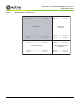
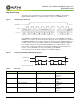
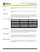
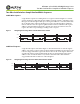
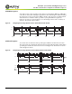
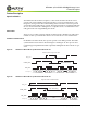
Table Of Contents
- 1/3-Inch Wide-VGA CMOS Digital Image Sensor
- Features
- Applications
- Ordering Information
- Table of Contents
- List of Figures
- List of Tables
- General Description
- Ball Descriptions
- Pixel Data Format
- Color Device Limitations
- Output Data Format
- Serial Bus Description
- Two-Wire Serial Interface Sample Read and Write Sequences
- Feature Description
- Operational Modes
- Signal Path
- On-Chip Biases
- Window Control
- Blanking Control
- Pixel Integration Control
- Variable ADC Resolution
- Gain Settings
- Black Level Calibration
- Row-wise Noise Correction
- Automatic Gain Control and Automatic Exposure Control
- Pixel Clock Speed
- Hard Reset of Logic
- Soft Reset of Logic
- STANDBY Control
- Monitor Mode Control
- Read Mode Options
- LINE_VALID
- LVDS Serial (Stand-Alone/Stereo) Output
- LVDS Output Format
- Electrical Specifications
- Package Dimensions
- Appendix A – Serial Configurations
- Appendix B – Power-On Reset and Standby Timing
- Revision History

PDF: 3295348826/Source:7478516499 Aptina reserves the right to change products or specifications without notice.
MT9V022_DS - Rev.H 6/10 EN
13 ©2005 Aptina Imaging Corporation. All rights reserved.
MT9V022: 1/3-Inch Wide-VGA Digital Image Sensor
Output Data Format
Output Data Timing
The data output of the MT9V022 is synchronized with the PIXCLK output. When
LINE_VALID is HIGH, one 10-bit pixel datum is output every PIXCLK period.
Figure 7: Timing Example of Pixel Data
The PIXCLK is a nominally inverted version of the master clock (SYSCLK). This allows
PIXCLK to be used as a clock to latch the data. However, when column bin 2 is enabled,
the PIXCLK is HIGH for one complete master clock master period and then LOW for one
complete master clock period; when column bin 4 is enabled, the PIXCLK is HIGH for
two complete master clock periods and then LOW for two complete master clock
periods. It is continuously enabled, even during the blanking period. Setting R0x74
bit[4] = 1 causes the MT9V022 to invert the polarity of the PIXCLK.
The parameters P1, A, Q, and P2 in Figure 8 are defined in Table 4.
Figure 8: Row Timing and FRAME_VALID/LINE_VALID Signals
Table 4: Frame Time
Parameter Name Equation Default Timing at 26.66 MHz
A Active data time R0x04 752 pixel clocks
= 752 master
= 28.20μs
P1 Frame start blanking R0x05 - 23 71 pixel clocks
= 71master
= 2.66μs
P2 Frame end blanking 23 (fixed) 23 pixel clocks
= 23 master
= 0.86μs
Q Horizontal blanking R0x05 94 pixel clocks
= 94 master
= 3.52μs
LINE_VALID
PIXCLK
D
OUT(9:0)
P
0
(9:0)
P
1
(9:0)
P2
(9:0)
P
3
(9:0)
P
4
(9:0)
P
n-1
(9:0)
P
n
(9:0)
Valid Image DataBlanking Blanking
...
...
...
...
P1 A Q A Q A P2
Number of master clocks
FRAME_VALID
LINE_VALID
...
...
...