
Datasheet-1
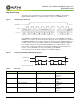
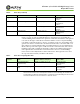
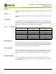
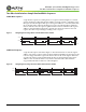
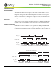
Table Of Contents
- 1/3-Inch Wide-VGA CMOS Digital Image Sensor
- Features
- Applications
- Ordering Information
- Table of Contents
- List of Figures
- List of Tables
- General Description
- Ball Descriptions
- Pixel Data Format
- Color Device Limitations
- Output Data Format
- Serial Bus Description
- Two-Wire Serial Interface Sample Read and Write Sequences
- Feature Description
- Operational Modes
- Signal Path
- On-Chip Biases
- Window Control
- Blanking Control
- Pixel Integration Control
- Variable ADC Resolution
- Gain Settings
- Black Level Calibration
- Row-wise Noise Correction
- Automatic Gain Control and Automatic Exposure Control
- Pixel Clock Speed
- Hard Reset of Logic
- Soft Reset of Logic
- STANDBY Control
- Monitor Mode Control
- Read Mode Options
- LINE_VALID
- LVDS Serial (Stand-Alone/Stereo) Output
- LVDS Output Format
- Electrical Specifications
- Package Dimensions
- Appendix A – Serial Configurations
- Appendix B – Power-On Reset and Standby Timing
- Revision History

PDF: 3295348826/Source:7478516499 Aptina reserves the right to change products or specifications without notice.
MT9V022_DS - Rev.H 6/10 EN
18 ©2005 Aptina Imaging Corporation. All rights reserved.
MT9V022: 1/3-Inch Wide-VGA Digital Image Sensor
Two-Wire Serial Interface Sample Read and Write Sequences
8-Bit Write Sequence
To be able to write 1 byte at a time to the register a special register address is added. The
8-bit write is done by first writing the upper 8 bits to the desired register and then writing
the lower 8 bits to the special register address (R0xF0). The register is not updated until
all 16 bits have been written. It is not possible to just update half of a register. In
Figure 11 on page 18, a typical sequence for 8-bit writing is shown. The second byte is
written to the special register (R0xF0).
Figure 11: Timing Diagram Showing a Bytewise Write to R0x09 with the Value 0x0284
8-Bit Read Sequence
To read one byte at a time the same special register address is used for the lower byte.
The upper 8 bits are read from the desired register. By following this with a read from the
special register (R0xF1) the lower 8 bits are accessed (Figure 12). The master sets the no-
acknowledge bits shown.
Figure 12: Timing Diagram Showing a Bytewise Read from R0x09; Returned Value 0x0284
STOP
R0xF0
ACKSTART
0xB8 ADDR
ACK
S
DATA
SCLK
ACKACKACKACK
R0x090xB8 ADDR
0000 0010 1000 0100
START
START
0xB9 ADDR
S
DATA
SCLK
STOP
NACK
ACKACKACK
R0x09
START
0xB8 ADDR
0000 0010
START
0xB9 ADDR
S
DATA
SCLK
NACKACKACKACK
R0xF0
START
0xB8 ADDR 1000 0100