
Datasheet-1
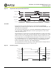
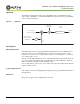
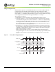
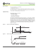
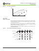
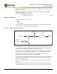
Table Of Contents
- 1/3-Inch Wide-VGA CMOS Digital Image Sensor
- Features
- Applications
- Ordering Information
- Table of Contents
- List of Figures
- List of Tables
- General Description
- Ball Descriptions
- Pixel Data Format
- Color Device Limitations
- Output Data Format
- Serial Bus Description
- Two-Wire Serial Interface Sample Read and Write Sequences
- Feature Description
- Operational Modes
- Signal Path
- On-Chip Biases
- Window Control
- Blanking Control
- Pixel Integration Control
- Variable ADC Resolution
- Gain Settings
- Black Level Calibration
- Row-wise Noise Correction
- Automatic Gain Control and Automatic Exposure Control
- Pixel Clock Speed
- Hard Reset of Logic
- Soft Reset of Logic
- STANDBY Control
- Monitor Mode Control
- Read Mode Options
- LINE_VALID
- LVDS Serial (Stand-Alone/Stereo) Output
- LVDS Output Format
- Electrical Specifications
- Package Dimensions
- Appendix A – Serial Configurations
- Appendix B – Power-On Reset and Standby Timing
- Revision History

PDF: 3295348826/Source:7478516499 Aptina reserves the right to change products or specifications without notice.
MT9V022_DS - Rev.H 6/10 EN
22 ©2005 Aptina Imaging Corporation. All rights reserved.
MT9V022: 1/3-Inch Wide-VGA Digital Image Sensor
Feature Description
Figure 17: Snapshot Mode Frame Synchronization Waveforms
Slave Mode
In slave mode, the exposure and readout are controlled using the EXPOSURE,
STFRM_OUT, and STLN_OUT pins. When the slave mode is enabled, STFRM_OUT and
STLN_OUT become input pins.
The start and end of integration are controlled by EXPOSURE and STFRM_OUT pulses,
respectively. While a STFRM_OUT pulse is used to stop integration, it is also used to
enable the readout process.
After integration is stopped, the user provides STLN_OUT pulses to trigger row readout.
A full row of data is read out with each STLN_OUT pulse. The user must provide enough
time between successive STLN_OUT pulses to allow the complete readout of one row.
It is also important to provide additional STLN_OUT pulses to allow the sensors to read
the vertical blanking rows. It is recommended that the user program the vertical blank
register (R0x06) with a value of 4, and achieve additional vertical blanking between
frames by delaying the application of the STFRM_OUT pulse.
The elapsed time between the rising edge of STLN_OUT and the first valid pixel data is
[horizontal blanking register (R0x05) + 4] clock cycles.
Figure 18: Slave Mode Operation
LED_OUT
D
OUT
(9:0)
LINE_VALID
FRAME_VALID
Exposure Time
xxx xxx xxx
EXPOSURE
1-ro w
time
2 master
clocks
1-ro w
time
98 master
clocks
Exposure
(input)
STFRM_OUT
(input)
LED_OUT
(output)
STLN_OUT
(input)
LINE_VALID
(output)
Integration T ime
Vertical Blanking
(def = 45 lines)