
Datasheet-1
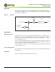
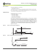
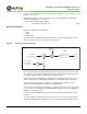
Table Of Contents
- 1/3-Inch Wide-VGA CMOS Digital Image Sensor
- Features
- Applications
- Ordering Information
- Table of Contents
- List of Figures
- List of Tables
- General Description
- Ball Descriptions
- Pixel Data Format
- Color Device Limitations
- Output Data Format
- Serial Bus Description
- Two-Wire Serial Interface Sample Read and Write Sequences
- Feature Description
- Operational Modes
- Signal Path
- On-Chip Biases
- Window Control
- Blanking Control
- Pixel Integration Control
- Variable ADC Resolution
- Gain Settings
- Black Level Calibration
- Row-wise Noise Correction
- Automatic Gain Control and Automatic Exposure Control
- Pixel Clock Speed
- Hard Reset of Logic
- Soft Reset of Logic
- STANDBY Control
- Monitor Mode Control
- Read Mode Options
- LINE_VALID
- LVDS Serial (Stand-Alone/Stereo) Output
- LVDS Output Format
- Electrical Specifications
- Package Dimensions
- Appendix A – Serial Configurations
- Appendix B – Power-On Reset and Standby Timing
- Revision History

PDF: 3295348826/Source:7478516499 Aptina reserves the right to change products or specifications without notice.
MT9V022_DS - Rev.H 6/10 EN
23 ©2005 Aptina Imaging Corporation. All rights reserved.
MT9V022: 1/3-Inch Wide-VGA Digital Image Sensor
Feature Description
Signal Path
The MT9V022 signal path consists of a programmable gain, a programmable analog
offset, and a 10-bit ADC. See “Black Level Calibration” on page 30 for the programmable
offset operation description.
Figure 19: Signal Path
On-Chip Biases
ADC Voltage Reference
The ADC voltage reference is programmed through R0x2C, bits 2:0. The ADC reference
ranges from 1.0V to 2.1V. The default value is 1.4V. The increment size of the voltage
reference is 0.1V from 1.0V to 1.6V (R0x2C[2:0] values 0 to 6). At R0x2C[2:0] = 7, the refer-
ence voltage jumps to 2.1V.
The effect of the ADC calibration does not scale with V
REF. Instead it is a fixed value rela-
tive to the output of the analog gain stage. At default, one LSB of calibration equals two
LSB in output data (1LSB
Offset
= 2mV, 1LSB
ADC
= 1mV).
It is very important to preserve the correct values of the other bits in R0x2C. The default
register setting is 0x0004.
V_Step Voltage Reference
This voltage is used for pixel high dynamic range operations, programmable from R0x31
through R0x34.
Chip Version
Chip version registers R0x00 and R0xFF are read-only.
Pixel Output
(reset minus signal)
Offset Correction
Voltage (R0x48 or
result of BLC)
10 (12) bit ADC
ADC Data
(9:0)
Gain Selection
(R0x35 or
result of AGC)
V
REF
(R0x2C)
C2
C1
S