
Datasheet-1
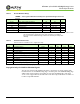
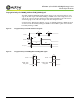
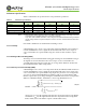
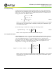
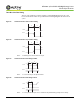
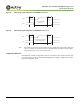

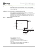
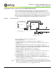
Table Of Contents
- 1/3-Inch Wide-VGA CMOS Digital Image Sensor
- Features
- Applications
- Ordering Information
- Table of Contents
- List of Figures
- List of Tables
- General Description
- Ball Descriptions
- Pixel Data Format
- Color Device Limitations
- Output Data Format
- Serial Bus Description
- Two-Wire Serial Interface Sample Read and Write Sequences
- Feature Description
- Operational Modes
- Signal Path
- On-Chip Biases
- Window Control
- Blanking Control
- Pixel Integration Control
- Variable ADC Resolution
- Gain Settings
- Black Level Calibration
- Row-wise Noise Correction
- Automatic Gain Control and Automatic Exposure Control
- Pixel Clock Speed
- Hard Reset of Logic
- Soft Reset of Logic
- STANDBY Control
- Monitor Mode Control
- Read Mode Options
- LINE_VALID
- LVDS Serial (Stand-Alone/Stereo) Output
- LVDS Output Format
- Electrical Specifications
- Package Dimensions
- Appendix A – Serial Configurations
- Appendix B – Power-On Reset and Standby Timing
- Revision History

PDF: 3295348826/Source:7478516499 Aptina reserves the right to change products or specifications without notice.
MT9V022_DS - Rev.H 6/10 EN
45 ©2005 Aptina Imaging Corporation. All rights reserved.
MT9V022: 1/3-Inch Wide-VGA Digital Image Sensor
Electrical Specifications
Two-Wire Serial Bus Timing
The two-wire serial bus operation requires certain minimum master clock cycles
between transitions. These are specified in the following diagrams in master clock
cycles.
Figure 37: Serial Host Interface Start Condition Timing
Figure 38: Serial Host Interface Stop Condition Timing
Notes: 1. All timing are in units of master clock cycle.
Figure 39: Serial Host Interface Data Timing for Write
Notes: 1. SDATA is driven by an off-chip transmitter.
Figure 40: Serial Host Interface Data Timing for Read
Notes: 1. SDATA is pulled LOW by the sensor, or allowed to be pulled HIGH by a pull-up resistor off-chip.
SCLK
4
S
DATA
4
SCLK
4
S
DATA
4
SCLK
4
S
DATA
4
SCLK
5
S
DATA