
Datasheet-1


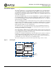


Table Of Contents
- 1/3-Inch Wide-VGA CMOS Digital Image Sensor
- Features
- Applications
- Ordering Information
- Table of Contents
- List of Figures
- List of Tables
- General Description
- Ball Descriptions
- Pixel Data Format
- Color Device Limitations
- Output Data Format
- Serial Bus Description
- Two-Wire Serial Interface Sample Read and Write Sequences
- Feature Description
- Operational Modes
- Signal Path
- On-Chip Biases
- Window Control
- Blanking Control
- Pixel Integration Control
- Variable ADC Resolution
- Gain Settings
- Black Level Calibration
- Row-wise Noise Correction
- Automatic Gain Control and Automatic Exposure Control
- Pixel Clock Speed
- Hard Reset of Logic
- Soft Reset of Logic
- STANDBY Control
- Monitor Mode Control
- Read Mode Options
- LINE_VALID
- LVDS Serial (Stand-Alone/Stereo) Output
- LVDS Output Format
- Electrical Specifications
- Package Dimensions
- Appendix A – Serial Configurations
- Appendix B – Power-On Reset and Standby Timing
- Revision History

PDF: 3295348826/Source:7478516499 Aptina reserves the right to change products or specifications without notice.
MT9V022_DS - Rev.H 6/10 EN
9 ©2005 Aptina Imaging Corporation. All rights reserved.
MT9V022: 1/3-Inch Wide-VGA Digital Image Sensor
Ball Descriptions
Notes: 1. Pin H7 (RSVD) must be tied to GND.
2. Output Enable (OE) tri-states signals D
OUT0–DOUT9. No other signals are tri-stated with OE.
3. No connect. These pins must be left floating for proper operation.
Figure 3: Typical Configuration (Connection)—Parallel Output Mode
Note: LVDS signals are to be left floating.
A2 SER_DATAOUT_P Output Serial data out (differential positive).
B4, E2 V
DD Supply Digital power 3.3V.
C8, F7 V
AA Supply Analog power 3.3V.
B8 VAAPIX Supply Pixel power 3.3V.
A1, A4 V
DDLVDS Supply Dedicated power for LVDS pads.
B1, C3 LVDSGND Ground Dedicated GND for LVDS pads.
C6, F3 D
GND Ground Digital GND.
C7, F6 A
GND Ground Analog GND.
E7, E8, D7, D8 NC NC No connect. 3
Table 3: Ball Descriptions (continued)
Only pins DOUT0 through DOUT9 may be tri-stated.
52-Ball IBGA
Numbers Symbol Type Description Note
SYSCLK
LINE_VALID
FRAME_VALID
PIXCLK
D
OUT(9:0)
STANDBY
EXPOSURE
RSVD
S_CTRL_ADR0
S_CTRL_ADR1
LVDSGND
LED_OUT
ERROR
S
DATA
SCLK
RESET#
OE
V
DDLVDS
A
GNDDGND
VDD VAA
VAAPIX
Master Clock
0.1mF
To Controller
STANDBY from
Controller or
Digital GND
Two-Wire
Serial Interface
V
DD
VAA VAAPIX
To LED output
10K
Ω
1.5K
Ω