
Datasheet

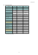
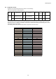
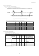
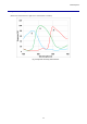
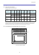
Table Of Contents
- Description
- Features
- Device Structure
- USE RESTRICTION NOTICE
- 1. Block Diagram and Pin Configuration
- 2. Pixel Signal Output Specifications
- 3. Control Registers
- 3-1 2-wire Serial Communication Operation Specifications
- 3-2 2-wire Serial Communication Register Map (Configuration register, Parameter limit register)
- 3-3 Parameter Limit Registers – [0x1000-0x1FFF] (Read Only and Static)
- 3-4 Manufacturer Specific Registers – [0x3000-0x5FFF ]
- 3-5 Frame Bank A and Bank B specific output samples
- 4. Output Data Format
- 6. On Chip Image Processing
- 7. NVM Memory Map
- 8. How to operate IMX219PQH5-C
- 9. Other Functions
- 10. Electrical Characteristics
- 11. Spectral Sensitivity Characteristic
- 12. Image Sensor Characteristics
- 13. Measurement Method for Image Sensor Characteristics
- 14. Spot Pixel Specification
- 15. Notice on White Pixels Specifications
- 16. Chief Ray Angle Characteristics
- 17. Connection Example
- 18. Notes On Handling

IMX219PQH5-C
84
10. Electrical Characteristics
10-1 Absolute Maximum Ratings
Table 41 Absolute Maximum Ratings
Item
Symbol
Min.
Typ.
Max.
Unit
Remarks
Supply voltage (analogue)
V
ANA
-0.3
3.3
V
Supply voltage (Core)
V
DDL
-0.3
2.0
V
Supply voltage (IF)
V
DIG
-0.3
3.3
V
Input voltage
V
I
-0.3
3.3
V
Output voltage
V
O
-0.3
3.3
V
Operating temperature (function)
Topr
-20
60
Junction temperature
Storage temperature
Tstg
-30
80
Junction temperature
Performance guarantee temperature
Tspec
-20
60
Junction temperature
10-2 Recommended Operating Conditions
Table 42 Recommended Operating Conditions
Item
Symbol
Min.
Typ.
Max.
Unit
Remarks
Supply voltage (analogue)
V
ANA
2.6
2.8
3.0
V
Supply voltage (Core)
V
DDL
1.08
1.2 1.3
V
Supply voltage (IF)
V
DIG
1.62
1.8 1.98
V