
Datasheet
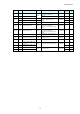
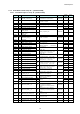
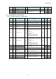
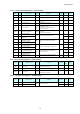
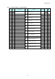
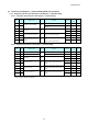
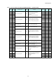
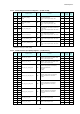
Table Of Contents
- Description
- Features
- Device Structure
- USE RESTRICTION NOTICE
- 1. Block Diagram and Pin Configuration
- 2. Pixel Signal Output Specifications
- 3. Control Registers
- 3-1 2-wire Serial Communication Operation Specifications
- 3-2 2-wire Serial Communication Register Map (Configuration register, Parameter limit register)
- 3-3 Parameter Limit Registers – [0x1000-0x1FFF] (Read Only and Static)
- 3-4 Manufacturer Specific Registers – [0x3000-0x5FFF ]
- 3-5 Frame Bank A and Bank B specific output samples
- 4. Output Data Format
- 6. On Chip Image Processing
- 7. NVM Memory Map
- 8. How to operate IMX219PQH5-C
- 9. Other Functions
- 10. Electrical Characteristics
- 11. Spectral Sensitivity Characteristic
- 12. Image Sensor Characteristics
- 13. Measurement Method for Image Sensor Characteristics
- 14. Spot Pixel Specification
- 15. Notice on White Pixels Specifications
- 16. Chief Ray Angle Characteristics
- 17. Connection Example
- 18. Notes On Handling

IMX219PQH5-C
31
Index
Byte
Register Name
RW
Comment
Re-Time
Default
(HEX)
Embd
DL
0x0170
[2:0]
X_ODD_INC_A
RW
x_odd_inc
Increment for odd pixels 1, 3
frame bank
1
0x0171
[2:0]
Y_ODD_INC_A
y_odd_inc
Increment for odd pixels 1, 3
frame bank
1
0x0172
[0]
IMG_ORIENTATION_A[0]
RW
image_orientation (for both direction)
bit[0]: hori. direction bit[1]: vert.
direction
frame bank
0
[1]
IMG_ORIENTATION_A[1]
RW
0
0x0173
Reserved
0x0174
[1:0]
BINNING_MODE_H_A
RW
defines binning mode (H-direction).
0: no-binning, 1: x2-binning,
2: x4-binning, 3: x2-analog (special)
binning
frame bank
0
0x0175
[1:0]
BINNING_MODE_V_A
RW
defines binning mode (V-direction).
0: no-binning, 1: x2-binning,
2: x4-binning, 3: x2-analog (special)
binning
frame bank
0
0x0176
[0]
BINNING_CAL_MODE_H_A
RW
defines binning mode (H-direction).
0 :average, 1: sum
frame bank
0
0x0177
[0]
BINNING_CAL_MODE_V_A
RW
defines binning mode (V-direction).
0: average, 1: sum
frame bank
0
0x0189
[7:0]
ANA_GAIN_GLOBAL_SHORT
_A
RW
Analog gain (short exposure)
frame bank
00
0x018A
[7:0]
COARSE_INTEG_TIME_SHO
RT_A [15:8]
RW
Coarse integ time (short exposure)
frame bank
01
0x018B
[7:0]
COARSE_INTEG_TIME_SHO
RT_A [7:0]
F4
0x018C
[7:0]
CSI_DATA_FORMAT_A [15:8]
RW
CSI-2 data format
frame bank
0A
0x018D
[7:0]
CSI_DATA_FORMAT_A [7:0]
0A