
12MP IMX477 Mini High Quality Camera Module for Raspberry Pi - Datasheet


IMX477-AACK-C
9
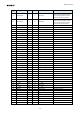
3. Pin Description
Table 1 Pin Description
Pin
No.
Symbol I/O A/D Pin description Remarks
A2 XVS I/O D
Digital I/O
(Vertical sync signal)
Used as a vertical synchronizing
signal of dual sensor application
A3 GYINT I D Digital input
Digital GND
(When using OIS combined system,
this pin has the function of the Gyro
interrupt)
A4 SCK O D Digital output
NC
(When using OIS combined system,
this pin has the function of the Gyro
control clock)
A5 SDI I/O D Digital I/O
Digital GND
(When using OIS combined system,
this pin has the function of the Gyro
data input)
A6 V
DD
LCN1 Power D V
DIG
power supply
A7 SDA I/O D Digital I/O I
2
C communication data input/output
A8 SLASEL I D Digital input I
2
C slave address select (Pull-down)
A9 GPO O D Digital output
B1 V
DD
LSC1 Power D V
DIG
power supply
B2 V
SS
LSC1 GND D V
DIG
GND
B3 TEST3/SDIC I D Digital input
Digital GND
(When using OIS combined system,
this pin has the function of the SPI
Communication for OIS control)
B4 SCSB O D Digital output
NC
(When using OIS combined system,
this pin has the function of the Gyro
chip select)
B5 SDO O D Digital output
NC
(When using OIS combined system,
this pin has the function of the Gyro
data output)
B6 V
SS
LCN1 GND D V
DIG
GND
B7 SCL I/O D Digital I/O I
2
C communication clock input
B8 TENABLE I D Digital input NC (Pull-down)
B9 V
SS
LSC2 GND D V
DIG
GND
B10 V
DD
LSC2 Power D V
DIG
power supply
C1 V
DD
MIO1 Power D V
IF
power supply
C2 V
SS
LSC3 GND D V
DIG
GND
C3 V
DD
HSN1 Power A V
ANA
power supply
C4 V
SS
HSN1 GND A V
ANA
GND
C5 VRLRD Minus A Analog input
Capacitor connection
(see Figure 5. Peripheral Circuit
Diagram)
C6 VRL Minus A Analog input
Capacitor connection
(see Figure 5. Peripheral Circuit
Diagram)
C7 V
SS
HSN2 GND A V
ANA
GND
C8 VPI Power A Analog input
Capacitor connection
(see Figure 5. Peripheral Circuit
Diagram)