
Datasheet
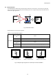
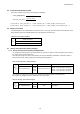
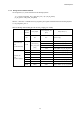
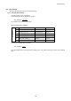
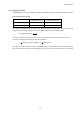
Table Of Contents
- Description
- Features
- Device Structure
- USE RESTRICTION NOTICE
- 1. Block Diagram and Pin Configuration
- 2. Pixel Signal Output Specifications
- 3. Control Registers
- 3-1 2-wire Serial Communication Operation Specifications
- 3-2 2-wire Serial Communication Register Map (Configuration register, Parameter limit register)
- 3-3 Parameter Limit Registers – [0x1000-0x1FFF] (Read Only and Static)
- 3-4 Manufacturer Specific Registers – [0x3000-0x5FFF ]
- 3-5 Frame Bank A and Bank B specific output samples
- 4. Output Data Format
- 6. On Chip Image Processing
- 7. NVM Memory Map
- 8. How to operate IMX219PQH5-C
- 9. Other Functions
- 10. Electrical Characteristics
- 11. Spectral Sensitivity Characteristic
- 12. Image Sensor Characteristics
- 13. Measurement Method for Image Sensor Characteristics
- 14. Spot Pixel Specification
- 15. Notice on White Pixels Specifications
- 16. Chief Ray Angle Characteristics
- 17. Connection Example
- 18. Notes On Handling

IMX219PQH5-C
51
The end of the address and register value is determined according to the tags embedded in the data.
Table 15 Embedded Data Line Tag
Tag
Data Byte Description
00h
Illegal Tag. If found treat as end of Data
07h
End of Data (Data Byte Value = 07H)
aah
CCI Register Index MSB [15:8]
a5h
CCI Register Index LSB [7:0]
5ah
Auto increment the CCI index after the data byte - valid data
Data byte contains valid CCI register data
55h
Auto increment the CCI index after the data byte - null data
A CCI register does NOT exist for the current CCI index.
The data byte value is the 07H
ffh
Illegal Tag. If found treat as end of Data