ArduCAM-M-2MP Camera Shield 2MP SPI Camera Hardware Application Note Rev 1.
ArduCAM-M-2MP Hardware Application Note Table of Contents 1 2 2.1 2.2 3 4 5 5.1 5.2 5.3 6 Introduction ............................................................................................................................. 2 Typical Wiring ......................................................................................................................... 2 Single Camera Wiring ........................................................................................................
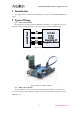
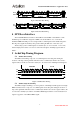
ArduCAM-M-2MP Hardware Application Note 1 Introduction This application note describes the detail hardware operation of ArduCAM-M-2MP camera shield. 2 Typical Wiring 2.1 Single Camera Wiring The typical connection between ArduCAM shield and Arduino or etc platform is shown in the Figure 1. More typically the Figure 2 shows the wiring for Arduino UNO R3 board. Figure 1 Typical Wiring Figure 2 Wiring for Arduino UNO R3 2.
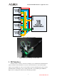
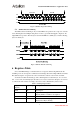
ArduCAM-M-2MP Hardware Application Note Figure 3 Multi-Cameras Wiring Figure 4 Mult-Cameras Wiring on Arduino UNO 3 I2C Interface The I2C interface is directly connected to the image sensor OV2640. The OV2640 I2C slave address is 0x60 for write and 0x61 for read. User can use I2C master to read and write all the registers in the OV2640 sensor. For more information about the OV2640 register, please refer the OV2640 datasheet. The Figure 5 shows writing value 0x01 to the OV2640 register 0xFF.
ArduCAM-M-2MP Hardware Application Note Figure 5 I2C Write Bus Timing Figure 6 I2C Read Bus Timing 4 SPI Slave Interface The ArduCAM SPI slave interface is fixed SPI mode 0 with POL = 0 and PHA = 1. The maximum speed of SCLK is designed for 8MHz, care should taken do not over clock the maximum 8MHz. The SPI protocol is designed with a command phase with variable data phase. The chip select signal should always keep asserted during the SPI read or write bus cycle.
ArduCAM-M-2MP Hardware Application Note Figure 8 SPI Bus Single Read Timing 5.3 SPI Bus Burst Read Timing The SPI bus burst read timing is only for burst FIFO read operation. It is composed of a burst read command phase and multiple data phases in order to get double throughput compared to the single FIFO read operation. The first byte read from the FIFO is a dummy byte, and the following bytes are valid bytes.
ArduCAM-M-2MP Hardware Application Note 0 = active high, 1 = active low Bit[1]: Sensor Vsync Polarity 0 = active high, 1 = active low Bit[3]: Sensor data delay 0 = no delay, 1= delay 1 PCLK Bit[4]: FIFO mode control 0 = FIFO mode disable, 1 = enable FIFO mode Bit[6]: low power mode control 0 = normal mode, 1 = low power mode 0x04 RW FIFO control Register Bit[0]: write ‘1’ to clear FIFO write done flag Bit[1]: write ‘1’ to start capture Bit[4]: write ‘1’ to reset FIFO write pointer Bit[5]: write ‘1’ to res