
User guide

Hardware Description
3-96 Copyright © 2003-2010 ARM Limited. All rights reserved. ARM DUI 0224I
3.22.1 JTAG and USB debug port support
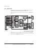
The PB926EJ-S supports debugging using embedded or external hardware. The
debugging interface can be controlled by:
JTAG hardware
The RealView Debugger and the AXD debugger, for example, use an
external interface box, such as RealView ICE or Multi-ICE, to connect to
the JTAG connector. If you are using an external JTAG debug tool, the
embedded debug hardware is disabled.
USB debug port
The USB debug port is embedded on the PB926EJ-S. An application,
Progcards or the RealView Debugger, for example, can control the JTAG
signals from the USB port of the PC. The PC and the PB926EJ-S are
connected by a standard USB cable.
Note
ARM Multi-ICE and RealView ICE ground pin 20 of the JTAG connector. On the
PB926EJ-S, pin 20 is connected to a pull-up resistor and the nICEDETECT signal.
The USB debug port is automatically disabled if a JTAG emulator is connected and
nICEDETECT is LOW. If you are using third-party debugging hardware, ensure that
a ground is present on pin 20 of the JTAG connector.
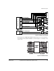
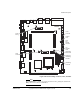
The PB926EJ-S has two scan chains:
Debug The D_x signals are used for the development chip and synthesized JTAG
TAP controllers in the RealView Logic Tile. This is the normal mode of
operation (see JTAG debug (normal) mode).
Config The C_x signals are used to program the FPGA and PLDs. This chain is
available in configuration mode (see JTAG configuration mode on
page 3-97). See also ChipScope integrated logic analyzer on page 3-104.
JTAG debug (normal) mode
During normal operation and software development, the PB926EJ-S operates in debug
mode.
The debug mode is selected by default (when a jumper is not fitted on the CONFIG link,
see Figure 3-42 on page 3-95). In debug mode:
• the signal nCFGEN is HIGH
• the CONFIG LED is off on the PB926EJ-S (and on each tile in the stack)