
User guide

Programmer’s Reference
ARM DUI 0224I Copyright © 2003-2010 ARM Limited. All rights reserved. 4-3
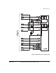
4.1 Memory map
The locations for memory, peripherals, and controllers are listed in Table 4-1 and ARM
Data bus memory map on page 4-8.
There are multiple buses in the ARM926EJ-S PXP Development Chip. Not all of the
buses can access all of the memory regions. See AHB bridges and the bus matrix on
page 3-10 and the ARM926EJ-S Reference Manual for details on the bus matrix and bus
accesses.
Note
The MOVE and VFP coprocessors are not memory-mapped peripherals so they do not
appear in the memory map listed in Table 4-1. See the appropriate technical reference
manual for more detail on these devices.
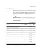
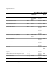
Table 4-1 Memory map
Peripheral Location
Interrupt
a
PIC
and SIC
Address
Region
size
MPMC Chip Select 0. Normally the bottom 64MB of the
first bank of SDRAM (During boot remapping, this can be
NOR flash or memory on a RealView Logic Tile.)
Board -
0x00000000–
0x03FFFFFF
64MB
MPMC Chip Select 0, top 64MB of the first bank of
SDRAM
Board -
0x04000000–
0x07FFFFFF
64MB
MPMC Chip Select 1, dynamic expansion memory Memory
expansion
-
0x08000000–
0x0FFFFFFF
128MB
System registers FPGA -
0x10000000–
0x10000FFF
4KB
PCI controller configuration registers FPGA -
0x10001000–
0x10001FFF
4KB
Serial Bus Interface FPGA -
0x10002000–
0x10002FFF
4KB
Secondary Interrupt Controller (SIC) FPGA PIC 31
0x10003000–
0x10003FFF
4KB
Advanced Audio CODEC Interface FPGA PIC24, SIC 24
0x10004000–
0x10004FFF
4KB