
User guide

Programmer’s Reference
4-32 Copyright © 2003-2010 ARM Limited. All rights reserved. ARM DUI 0224I
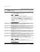
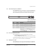
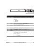
Figure 4-13 SYS_MCI
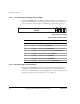
4.3.12 Flash Control Register, SYS_FLASH
Bit 0 of the SYS_FLASH register at
0x1000004C
controls write protection of NOR flash
devices. The function of the register bits are shown in Table 4-13.
4.3.13 CLCD Control Register, SYS_CLCD
The SYS_CLCD register at
0x10000050
controls LCD power and multiplexing and
controls the interface to the touchscreen as listed in Table 4-14 on page 4-33. See also
LCD power control on page C-7.
Table 4-12 MCI control
Bits Access Description
[31:5] - Reserved. Use read-modify-write to preserve value.
[4] - Reserved (data multiplex)
[3] Read Write protect 1
[2] Read Write protect 0
[1] Read Card detect 1
[0] Read Card detect 0
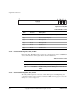
Table 4-13 Flash control
Bits Access Description
[31:1] - Reserved. Use read-modify-write to preserve value.
[0] Read/write Disables writing to flash if LOW (power-on reset state is
LOW)