
User guide

Programmer’s Reference
4-86 Copyright © 2003-2010 ARM Limited. All rights reserved. ARM DUI 0224I
4.19 Serial bus interface
A serial bus interface is implemented in the FPGA. The registers shown in Table 4-61
control the serial bus and provides access to control signals on the two memory
expansion boards and to the time-of-year clock.
Note
SDA is an open-collector signal that is used for sending and receiving data. Set the
output value HIGH before reading the current value.
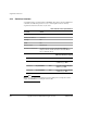
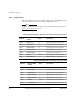
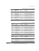
Table 4-60 Serial bus implementation
Property Value
Location FPGA
Memory base address
0x10002000
Interrupt NA
DMA NA
Release version Custom logic
Reference documentation Serial bus interface on page 3-80, Appendix E Memory
Expansion Boards, and the datasheet for the Dallas Maxim
DS1338 Real Time Clock.
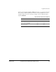
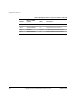
Table 4-61 Serial bus register
Address Name Access Description
0x10002000
SB_CONTROL Read Read serial control bits: Bit [0]
is SCL Bit [1] is SDA
0x10002000
SB_CONTROLS Write Set serial control bits: Bit [0] is
SCL Bit [1] is SDA
0x10002004
SB_CONTROLC Write Clear serial control bits: Bit [0]
is SCL Bit [1] is SDA